High Electron Mobility Transistors
Mastering the Technology Behind Next-Generation High-Speed Electronics
Navigate the sophisticated world of High Electron Mobility Transistors and discover how these remarkable devices power the fastest, most efficient electronics in the world.
238 pages11 chaptersJul 2, 2026Semiconductors
About this book
This comprehensive guide takes you from fundamental physics principles through practical design and implementation strategies. You'll explore the heterostructure engineering that makes HEMTs possible, understand the two-dimensional electron gas that gives these transistors their exceptional speed, and learn how to select the right material systems for your specific application. Whether you're designing RF amplifiers, power converters, or millimeter-wave circuits, this book provides the technical depth and practical insights needed to optimize HEMT performance. Discover real-world challenges including thermal management, parasitic effects, and reliability considerations that separate theoretical knowledge from successful implementation. With clear explanations of complex concepts and actionable guidance for device design and fabrication, you'll gain the expertise to leverage HEMT technology for cutting-edge applications.
Table of contents
- IntroductionWhy HEMTs Matter in Modern Electronics, Your Roadmap Through This Book, Key Concepts You'll MasterRead below
- Chapter 1: Fundamentals of Semiconductor PhysicsEnergy Band Structure and Electron Behavior, Carrier Transport and Mobility, Introduction to Heterostructures
- Chapter 2: The Two-Dimensional Electron GasHow the 2DEG Forms at Heterointerfaces, Properties and Characteristics of the 2DEG, Quantum Confinement Effects
- Chapter 3: HEMT Device Structure and DesignBasic HEMT Architecture, Designing the Heterostructure Layers, Gate Engineering and Contact Design, Doping Profiles and Electron Confinement
- Chapter 4: Material Systems for HEMTsGaAs-Based HEMT Systems, GaN-Based HEMTs for Power Applications, InP and InGaAs Systems for Ultra-High Frequency, Selecting the Right Material for Your Application
- Chapter 5: HEMT Operation and Electrical CharacteristicsDC Performance and I-V Characteristics, AC Performance and Frequency Response, Transconductance and Gain Mechanisms
- Chapter 6: Fabrication and ProcessingEpitaxial Growth Techniques, Lithography and Etching Processes, Metallization and Contact Formation, Process Control and Quality Assurance
- Chapter 7: RF and Microwave ApplicationsRF Amplifier Design and Optimization, Microwave Circuit Applications, Millimeter-Wave and Terahertz Applications
- Chapter 8: Power Electronics and High-Voltage ApplicationsPower Switching and Efficiency, Thermal Management in Power HEMTs, Reliability and Long-Term Performance
- Chapter 9: Parasitic Effects and Device LimitationsParasitic Capacitances and Resistances, Current Collapse and Trapping Effects, Dispersion and Frequency-Dependent Behavior
- Chapter 10: Modeling and SimulationCompact Models for Circuit Design, Physics-Based Simulation Approaches, Parameter Extraction and Model Validation
- Chapter 11: Future Trends and Emerging TechnologiesWide-Bandgap Semiconductors and Beyond, Advanced Device Architectures, Integration Challenges and Solutions
- ConclusionKey Takeaways and Next Steps, Continuing Your HEMT Journey
- Glossary of Terms
- Further Reading and Resources
Introduction
Every time a satellite phone connects across thousands of miles, every time a radar system tracks an aircraft at altitude, and every time a 5G base station handles thousands of simultaneous connections, there is a small but extraordinary device doing the heavy lifting. That device is the High Electron Mobility Transistor, or HEMT. It is not a household name, but it is one of the most consequential inventions in the history of semiconductor electronics. Without it, the high-frequency, high-speed world we now take for granted simply would not exist in its current form.
HEMTs emerged from a fundamental insight in semiconductor physics: if you could separate electrons from the atoms that donate them, those electrons would move far more freely through a crystal lattice. That insight, realized in the late 1970s and early 1980s through the engineering of layered semiconductor structures called heterostructures, produced a transistor capable of operating at frequencies and efficiencies that conventional silicon devices could not approach. The physics behind this is elegant, and understanding it opens up a powerful toolkit for designing electronics that push the boundaries of what is possible.
This book is written for engineers and semiconductor professionals who already have a working knowledge of electronics and want to go deeper. You may have encountered HEMTs in a datasheet, in a circuit design context, or in a research paper. You may be designing RF amplifiers, working on power conversion systems, or exploring millimeter-wave applications. Whatever your starting point, this book is structured to take you from the foundational physics all the way through to practical design, fabrication, and real-world application. The goal is not just to explain what HEMTs are, but to give you the understanding and tools to work with them confidently and effectively.
The field of HEMT technology is broad and moves quickly. New material systems, device architectures, and fabrication techniques continue to expand what these transistors can do. Gallium nitride HEMTs are transforming power electronics. Indium phosphide-based devices are pushing frequency limits into the terahertz range. Wide-bandgap materials are enabling power densities that were unimaginable a decade ago. Staying current with these developments requires a solid grounding in the underlying principles, and that is exactly what this book provides. By the time you finish, you will have both the conceptual framework and the practical knowledge to engage with HEMT technology at a professional level.
Why HEMTs Matter in Modern Electronics
To appreciate why HEMTs matter, it helps to understand what conventional transistors struggle with at high frequencies. In a standard silicon MOSFET, electrons travel through a doped semiconductor channel. The dopant atoms that provide those electrons also scatter them, reducing their mobility and limiting how fast the device can switch. As operating frequencies climb into the gigahertz range, this scattering becomes a serious bottleneck. The transistor simply cannot respond fast enough, and its noise performance degrades significantly.
HEMTs solve this problem through a clever structural trick. By forming a junction between two semiconductor materials with different bandgaps, a quantum well is created at the interface. Electrons accumulate in this well, forming what is called a two-dimensional electron gas (2DEG). Because these electrons are spatially separated from the donor atoms, they experience far less scattering. The result is electron mobility that can be five to ten times higher than in comparable silicon devices, and in some material systems, even more.[1]
This mobility advantage translates directly into performance metrics that matter for real applications. Consider the following areas where HEMTs have become the device of choice:
- RF and microwave amplifiers: HEMTs deliver low noise figures and high gain at frequencies from 1 GHz to well above 100 GHz, making them essential in satellite communications, radar, and wireless infrastructure.
- Millimeter-wave systems: At frequencies above 30 GHz, HEMTs based on InP and GaAs are often the only practical transistor option for achieving the required gain and noise performance.
- Power electronics: GaN HEMTs can handle high voltages and currents while switching at high frequencies, enabling compact, efficient power converters for electric vehicles, data centers, and industrial systems.
- Defense and aerospace: Radar, electronic warfare, and satellite payloads rely heavily on HEMT-based monolithic microwave integrated circuits (MMICs) for their combination of performance and reliability.
The numbers behind HEMT performance are striking. A state-of-the-art InP HEMT can achieve a cutoff frequency (fT) exceeding 600 GHz, meaning it can amplify signals at frequencies approaching the terahertz range.[2] A GaN HEMT can deliver power densities of 10 W/mm or more at microwave frequencies, compared to roughly 1 W/mm for GaAs-based devices. These are not incremental improvements. They represent qualitative leaps in capability that open up entirely new application spaces.
Beyond raw performance, HEMTs matter because of where electronics is heading. The rollout of 5G and the development of 6G networks demand transistors that can operate efficiently at millimeter-wave frequencies. Autonomous vehicles require radar systems that work reliably at 77 GHz and above. Satellite constellations in low Earth orbit need compact, efficient amplifiers that can handle the thermal and radiation environment of space. In every one of these growth areas, HEMT technology is either already central or rapidly becoming so.
It is also worth noting that HEMT technology is not standing still. The transition from GaAs to GaN for power applications has already reshaped the power electronics industry. Research into aluminum nitride (AlN), gallium oxide (Ga2O3), and diamond-based heterostructures points toward a next generation of devices with even higher breakdown voltages and power densities. Understanding the principles behind current HEMTs is the foundation for engaging with these emerging technologies as they mature.
For engineers working in any of these domains, HEMT knowledge is no longer a niche specialty. It is becoming a core competency. Whether you are selecting a device for a circuit design, evaluating a process technology, or developing new device architectures, a deep understanding of how HEMTs work and why they behave the way they do is an essential professional asset.
Your Roadmap Through This Book
This book is organized to build your understanding progressively, starting from the physics that makes HEMTs possible and moving through device design, material systems, fabrication, applications, and finally to modeling and future directions. Each chapter is designed to stand on its own as a reference, but reading them in sequence will give you the most coherent picture of how all the pieces fit together.
Chapters 1 and 2 lay the physical foundation. Chapter 1 covers the semiconductor physics you need to understand HEMTs: energy band structure, carrier transport, and the concept of heterostructures. If you have a solid background in semiconductor physics, you may move through this chapter quickly, but it is worth reviewing because the specific concepts introduced here are referenced throughout the rest of the book. Chapter 2 then dives into the two-dimensional electron gas itself, explaining how it forms, what its properties are, and how quantum confinement shapes its behavior. This is the heart of HEMT physics, and time spent here pays dividends in every subsequent chapter.
Chapter 3 moves from physics to engineering, covering HEMT device structure and design. You will learn how the heterostructure layers are arranged, how the gate is engineered to control the 2DEG, and how doping profiles are used to optimize electron confinement. This chapter introduces the design trade-offs that every HEMT engineer faces, and it provides a framework for thinking about device optimization that applies across all material systems.
Chapter 4 surveys the major material systems used in HEMT technology. The three primary platforms are covered in detail:
- GaAs-based HEMTs: The original and still widely used platform for low-noise RF applications.
- GaN-based HEMTs: The dominant technology for high-power microwave and power electronics applications.
- InP and InGaAs systems: The leading platform for ultra-high-frequency and low-noise applications above 100 GHz.
The chapter concludes with a practical guide to selecting the right material system for a given application, covering the key trade-offs in frequency capability, power handling, noise performance, cost, and manufacturability.
Chapters 5 and 6 cover device operation and fabrication. Chapter 5 examines the electrical characteristics of HEMTs in detail, including DC behavior, frequency response, transconductance, and gain mechanisms. Chapter 6 then explains how these devices are actually made, covering epitaxial growth techniques, lithography, etching, metallization, and process control. Understanding fabrication is essential for anyone who needs to specify process requirements, interpret device variability, or troubleshoot performance issues.
Chapters 7 and 8 address the two major application domains for HEMTs. Chapter 7 covers RF and microwave applications, including amplifier design, microwave circuit integration, and millimeter-wave systems. Chapter 8 focuses on power electronics, covering switching performance, thermal management, and reliability. Both chapters are application-focused and include specific design guidance and real-world examples.
Chapters 9 and 10 tackle the more advanced topics of parasitic effects and device modeling. Chapter 9 examines the non-ideal behaviors that limit real HEMT performance, including parasitic capacitances and resistances, current collapse, trapping effects, and frequency-dependent dispersion. Chapter 10 covers the modeling and simulation tools used to predict and optimize HEMT behavior, from compact circuit models to physics-based simulation approaches and parameter extraction methods.
Chapter 11 looks ahead to the future of HEMT technology, covering wide-bandgap semiconductors beyond GaN, advanced device architectures, and the integration challenges that will shape the next generation of high-performance electronics. The book closes with a conclusion that synthesizes the key themes and points toward continued learning resources.
Key Concepts You'll Master
Before diving into the chapters, it is useful to preview the core concepts that run through the entire book. These are the ideas that, once understood deeply, unlock everything else. Think of them as the load-bearing pillars of HEMT knowledge. Each one is introduced gradually and built upon across multiple chapters, so this preview is meant to orient you rather than explain everything upfront.
The first and most fundamental concept is the heterostructure. A heterostructure is a layered semiconductor structure in which adjacent layers are made from different semiconductor materials. The key property that makes heterostructures useful is the band offset at the interface between two materials with different bandgaps. This band offset creates an energy discontinuity that can trap electrons in a very thin region, forming the quantum well that is central to HEMT operation. Understanding how band offsets arise, how they are engineered, and how they affect device behavior is essential throughout this book.
The second core concept is the two-dimensional electron gas (2DEG). The 2DEG is the channel through which current flows in a HEMT. It is called two-dimensional because the electrons are confined so tightly in the direction perpendicular to the heterointerface that they can only move freely in the two dimensions parallel to it. This confinement, combined with the separation from ionized dopants, is what gives the 2DEG its exceptional mobility. Key properties to understand include:
- Sheet carrier density (
ns): The number of electrons per unit area in the 2DEG, typically in the range of 1012 cm-2. - Electron mobility (
µ): How easily electrons move through the 2DEG under an applied electric field, measured in cm2/V·s. - Sheet resistance (
Rsh): The resistance of the 2DEG per square, which directly affects device on-resistance and power loss.
The third concept is transconductance (gm), which describes how effectively the gate voltage controls the drain current. Transconductance is the primary figure of merit for a transistor's amplification capability. In a HEMT, transconductance is closely linked to the 2DEG density and the gate-to-channel distance. Higher transconductance generally means higher gain, but it also comes with trade-offs in terms of linearity and noise. Understanding how to optimize transconductance for a specific application is one of the central design challenges in HEMT engineering.
The fourth concept is cutoff frequency (fT) and maximum oscillation frequency (fmax). These two figures of merit define the high-frequency limits of a transistor. fT is the frequency at which the current gain drops to unity, and it is primarily determined by the gate length and electron velocity in the channel. fmax is the frequency at which the power gain drops to unity, and it depends on both fT and the parasitic resistances and capacitances of the device. For most RF applications, fmax is the more practically relevant figure, but both are important for characterizing device performance.
A useful rule of thumb: for a HEMT to be useful in a circuit operating at frequency
f, you generally wantfTto be at least five to ten times higher thanf. This headroom ensures adequate gain and manageable noise performance in the operating band.
The fifth concept is material system selection. HEMTs are not made from a single material. They are built from combinations of semiconductors chosen to create the right band offsets, mobility characteristics, and physical properties for a given application. The choice of material system determines the frequency range, power handling capability, noise performance, and cost of the final device. GaAs, GaN, InP, and their alloys each have distinct strengths and limitations, and knowing how to match material properties to application requirements is a critical engineering skill.
The sixth concept is parasitic effects and their management. Real HEMTs are not ideal devices. They have parasitic capacitances at the gate, source, and drain that limit high-frequency performance. They have parasitic resistances in the contact regions and access regions that increase noise and reduce gain. They can suffer from current collapse, a phenomenon where trapping of electrons at surface states or in the buffer layer causes the drain current to drop below its expected value under RF drive conditions. Understanding these non-ideal effects and knowing how to mitigate them through design and process choices is what separates a working device from a high-performing one.
Finally, the concept of thermal management runs through the entire book, particularly in the context of power HEMTs. High-power devices generate significant heat, and the thermal resistance between the active region of the device and the heat sink determines how hot the channel gets during operation. Elevated channel temperatures accelerate degradation mechanisms and reduce device lifetime. GaN HEMTs, which operate at high power densities, are particularly sensitive to thermal management. Techniques for reducing thermal resistance, including substrate thinning, flip-chip bonding, and diamond heat spreaders, are covered in detail in the power electronics chapter.
These seven concepts form the conceptual backbone of this book. As you work through each chapter, you will see them appear repeatedly in different contexts and at increasing levels of depth. By the end, they will not just be abstract ideas. They will be practical tools that you can apply directly to your own design and engineering work. The goal is to give you not just knowledge about HEMTs, but genuine fluency with the technology, the kind that lets you look at a device specification, a process cross-section, or a circuit schematic and immediately understand what is happening and why.
This is the end of the free sample. The full book has 11 chapters.
Want this book written for you?
Tell us your goals and background, and get your own version of this book, tailored by AI to you.


Benefits of AI-tailored books
- Read one book, not ten:
- all the Semiconductors knowledge you need, gathered into a single book.
- Save days of learning:
- tell us your goals, choose your topics, and the whole book is built around them.
- Learn effortlessly:
- Semiconductors book written for your specific background and expertise.
- Understand at a glance:
- includes charts, tables, timelines, checklists, decision trees, and more.
- Stay current:
- written the day you order it, not years ago.
- Trust what you read:
- every book is checked for accuracy, with real research when your subject needs it.
Create your unique book in 3 steps
- 1. Select your focus
Select the focus of your Semiconductors book and share your background
- 2. Personalize your book
Specify your goals and choose sub-topics to include
- 3. Get your tailored book
Your book is ready in 10 minutes. Read it online, download as EPUB or PDF, or send to Kindle.


Frequently asked questions
- What is TailoredRead?
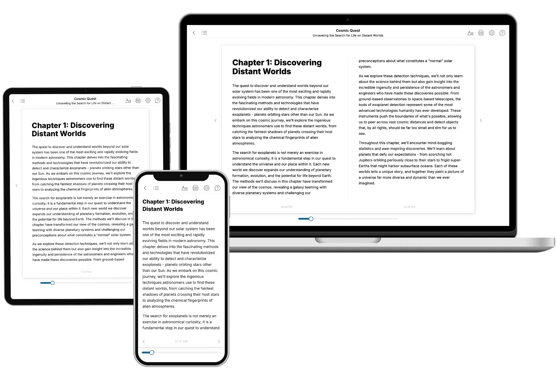
TailoredRead creates complete, full-length nonfiction ebooks, written specifically for you. Tell us what you want to learn and why, and TailoredRead writes you a complete ebook on it, with charts, tables, and diagrams throughout. Read it online, on Kindle, or on any e-reader, or download it as a PDF or EPUB. Every book is written fresh the day you order it.
- How is the book tailored to me?
Before anything is written, you answer a few short questions about your goals, your background, and the topics you care about. Your book is then planned around your answers: written at your level, focused on your goals, and covering the topics you chose, instead of the one-size-fits-all book a store sells everyone.
- Will it read like generic AI content?
No. Your book isn't a chat transcript: it's planned chapter by chapter before a single word is written, told in a clear book voice, and explains ideas visually with charts, tables, and diagrams. After writing, every book goes through an editorial pass that polishes chapters so the book reads consistent from start to finish. Judge for yourself: browse thousands of sample books on our Explore Books page.
- How accurate is the content?
Our AI first checks whether your subject needs live research. Niche and fast-moving subjects are researched before writing, and the book plan and chapters are grounded in what it finds. After writing, every book goes through a quality pass that checks its facts and consistency, and researched books list their sources in a Notes section at the back.
- How long is the book?
You choose the length: Comprehensive (250-300 pages), Detailed (150-200 pages), Essential (70-100 pages), or Short (30-50 pages).
- Does the book include visuals?
Yes. Every book includes charts, tables, and diagrams: timelines, checklists, step-by-step guides, decision trees, comparison tables, matrices, and bar charts. A typical book includes dozens of these visual elements.
- Can I read it on Kindle? What formats can I download?
Yes. Every book can be read in our online reader or downloaded as a PDF or EPUB. The EPUB can be opened with Kindle, Apple Books, Kobo, and any e-reader. The Commercial and Author licenses also include an editable Word (DOCX) and Markdown download.
- How much does it cost?
About the price of a regular ebook. The exact price depends on your book's length and complexity, from $2 for the shortest books to $35 for the most comprehensive, and it's shown when you review your book, before you commit to anything. Each book is a one-time purchase, yours to keep, no subscription. Licenses that let you share, teach, or publish your book range from $35.99 to $49.99.
- Can I preview the book before purchasing?
Before you pay, you'll see what your book will cover: the title, a detailed description, the estimated length, and the complete chapter-by-chapter table of contents, so you know what you're getting before you decide. The full text itself is written after you purchase.
- How long does it take to create a book?
About 10 minutes. You can start reading the opening chapters while the rest is still being written.