Photonic Crystals Explained
Mastering Light Control Through Engineered Materials
Discover how engineered materials can bend light to your will.
238 pages11 chaptersMay 10, 2026Photonics
About this book
This comprehensive guide takes you from fundamental principles to cutting-edge applications of photonic crystals—the revolutionary structures that control light propagation with unprecedented precision. You'll learn how photonic bandgaps work, explore the differences between one-, two-, and three-dimensional crystals, and understand the fabrication techniques that bring these structures to life. Whether you're interested in telecommunications, biosensing, or quantum photonics, this book provides the theoretical foundation and practical insights needed to design and implement photonic crystal solutions. With clear explanations, real-world examples, and accessible mathematics, you'll gain the knowledge to evaluate photonic crystal technologies and contribute to this rapidly evolving field. Perfect for researchers, engineers, and advanced students ready to master the science of light control.
Table of contents
- IntroductionWhy Photonic Crystals Matter, The Light Control Revolution, How to Use This Book, What You'll Learn and AccomplishRead below
- Chapter 1: Fundamentals of Light and Periodic StructuresProperties of Light and Electromagnetic Waves, Periodicity and Crystal Structures, How Light Interacts with Matter
- Chapter 2: The Photonic Bandgap ConceptFrom Electronic to Photonic Bandgaps, How Photonic Bandgaps Form, Bandgap Width and Frequency Ranges, Practical Implications of Bandgaps
- Chapter 3: One-Dimensional Photonic CrystalsStructure and Design Principles, Optical Properties and Behavior, Applications in Mirrors and Filters
- Chapter 4: Two-Dimensional Photonic CrystalsLattice Types and Symmetries, Engineering Bandgaps in 2D Structures, Waveguides and Cavities, Real-World 2D Photonic Crystal Examples
- Chapter 5: Three-Dimensional Photonic CrystalsStructural Complexity and Design, Complete Photonic Bandgaps, Fabrication Challenges and Solutions
- Chapter 6: Computational Modeling and SimulationSimulation Methods and Tools, Calculating Band Structures, Design Optimization Techniques, Available Software and Platforms
- Chapter 7: Fabrication Techniques and MethodsLayer Deposition and Thin Films, Lithography and Etching Processes, Advanced Nanofabrication Techniques
- Chapter 8: Defects, Cavities, and WaveguidesEngineering Defects Intentionally, Cavity Resonators and Quality Factors, Waveguide Design and Light Routing, Applications of Defect Engineering
- Chapter 9: Telecommunications and Integrated PhotonicsIntegration with Fiber Optics, Wavelength Filtering and Multiplexing, Photonic Integrated Circuits
- Chapter 10: Biosensing and Environmental MonitoringBiosensor Design Principles, Label-Free Detection Methods, Environmental Monitoring Applications, Enhancing Sensitivity and Specificity
- Chapter 11: Emerging Applications and Future DirectionsQuantum Photonics and Computing, Topological Photonics, Active and Dynamic Control Systems
- ConclusionKey Takeaways, Your Next Steps in Photonic Crystals
- Glossary
- Further Reading and Resources
Introduction
Light is one of the most fundamental forces shaping modern technology. From the fiber optic cables carrying internet traffic across continents to the lasers reading data from a disc, controlling how light behaves is at the heart of countless innovations. Yet for most of human history, our ability to manipulate light was limited to simple tools: lenses, mirrors, and prisms. These are powerful in their own right, but they work by bending or reflecting light rather than truly engineering its behavior at a fundamental level. Photonic crystals change that equation entirely.
A photonic crystal is a material with a carefully engineered periodic structure that controls which wavelengths of light can propagate through it and which cannot. The concept sounds deceptively simple, but the implications are profound. By designing the structure of a material at the nanoscale, engineers and physicists can create what is called a photonic bandgap: a range of frequencies that the material simply refuses to transmit. Light at those frequencies gets reflected, trapped, or redirected with a precision that no conventional optical component can match. This is not just a refinement of existing technology. It is a fundamentally new way of thinking about light.
The analogy that most physicists reach for is the semiconductor. In the mid-twentieth century, understanding how electrons behave in crystalline materials led to the transistor, the integrated circuit, and ultimately the entire digital revolution. Photonic crystals offer a parallel opportunity for light. Just as a semiconductor's periodic atomic lattice creates electronic bandgaps that allow engineers to control electron flow, a photonic crystal's periodic dielectric structure creates photonic bandgaps that allow engineers to control light flow. The potential consequences for computing, communications, sensing, and quantum technology are enormous, and the field is still young enough that many of the most exciting discoveries are still ahead.
This book is designed to take you from foundational principles to practical applications in a way that is rigorous without being impenetrable. Whether you are a physics student looking to specialize, an engineer exploring new materials, or a researcher branching into photonics, the goal is the same: to give you a clear, working understanding of how photonic crystals function and why they matter. The chapters ahead cover everything from the mathematics of bandgap formation to the fabrication techniques used in real laboratories, from computational modeling tools to cutting-edge applications in quantum computing and biosensing.
Why Photonic Crystals Matter
The question of why photonic crystals deserve serious attention comes down to a single practical reality: the demand for faster, more efficient, and more precise control of light is growing faster than conventional optics can keep up with. Telecommunications networks are pushing toward higher bandwidths. Medical diagnostics need sensors that can detect single molecules. Quantum computing requires components that can manipulate individual photons with near-perfect reliability. Photonic crystals are one of the most promising answers to all of these challenges simultaneously.
Consider the telecommunications industry as a concrete example. Modern fiber optic networks transmit data by encoding information onto light signals at specific wavelengths. To route these signals efficiently, networks need components that can filter, split, and redirect individual wavelengths without converting them to electrical signals and back again. That conversion process is slow and energy-intensive. Photonic crystal-based filters and waveguides can perform the same routing functions entirely in the optical domain, at speeds and energy efficiencies that electronic components simply cannot match.[1]
In biosensing, the stakes are equally high. Detecting a disease biomarker at extremely low concentrations in a blood sample requires a sensor with extraordinary sensitivity. Photonic crystal biosensors can detect shifts in resonant frequency caused by the binding of a single layer of molecules to a surface. This label-free detection capability, meaning no fluorescent tags or chemical markers are needed, makes photonic crystal sensors faster, cheaper, and more practical for point-of-care diagnostics than many competing technologies.
Beyond these established application areas, photonic crystals are opening doors in fields that barely existed a decade ago. Topological photonics, which borrows concepts from condensed matter physics to create light pathways that are immune to defects and disorder, relies heavily on photonic crystal structures. Quantum photonic circuits, which need to route single photons with minimal loss, use photonic crystal cavities and waveguides as their core building blocks. These are not distant future applications. Research groups around the world are demonstrating working devices right now.
It is also worth noting that photonic crystals are not purely a laboratory curiosity. Nature discovered them long before humans did. The iridescent wings of the Morpho butterfly, the shimmering colors of opal gemstones, and the structural coloration of certain beetle shells are all produced by naturally occurring photonic crystal structures.[2] These biological examples demonstrate that photonic crystal effects are robust, scalable, and achievable without exotic materials. They also provide inspiration for bio-inspired designs that researchers are actively exploring today.
Understanding photonic crystals also builds a broader intuition about how structured materials behave. The principles you will encounter in this book, periodicity, wave interference, bandgap formation, and defect engineering, appear across many areas of modern physics and engineering. Mastering these concepts in the context of photonic crystals gives you a transferable framework for thinking about phononic crystals (which control sound), plasmonic structures (which control surface waves), and metamaterials (which exhibit properties not found in nature). The investment in understanding photonic crystals pays dividends well beyond the field itself.
Finally, photonic crystals matter because the field is at an inflection point. Fabrication techniques have advanced to the point where structures that were theoretically predicted in the 1980s and 1990s can now be reliably manufactured. Computational tools have become powerful enough to design complex three-dimensional structures in hours rather than months. The gap between theory and practical implementation is narrowing rapidly, and the next decade is likely to see photonic crystal technologies move from research labs into mainstream products at an accelerating pace.
The Light Control Revolution
To appreciate what photonic crystals represent, it helps to understand the broader arc of humanity's relationship with light control. For centuries, optical technology advanced through the refinement of glass and the geometry of lenses. The telescope, the microscope, and the camera all emerged from this tradition. These tools are extraordinarily useful, but they work by exploiting the bulk properties of materials, primarily refractive index, rather than engineering the material's structure at the wavelength scale of light itself.
The modern era of light control began in earnest with the laser in 1960 and the development of fiber optics in the 1970s. These technologies gave engineers the ability to generate coherent light and transmit it over long distances with low loss. But even these advances relied on relatively simple material structures. A glass fiber guides light through total internal reflection, a phenomenon that depends on the refractive index difference between the fiber core and its cladding. The structure is elegant, but it offers limited ability to select specific wavelengths or manipulate light at the nanoscale.
The conceptual breakthrough that launched the photonic crystal revolution came in 1987, when two independent research groups, Eli Yablonovitch at Bell Communications Research and Sajeev John at Princeton University, published papers proposing that periodic dielectric structures could create complete photonic bandgaps.[3] Yablonovitch was motivated by the desire to suppress spontaneous emission in lasers to improve their efficiency. John was interested in the localization of light in disordered systems. Both arrived at the same fundamental insight: structure, not just composition, could be used to control light propagation in ways that bulk materials never could.
The years following those landmark papers saw an explosion of theoretical work. Researchers developed the mathematical tools needed to calculate photonic band structures, analogous to the electronic band structures used in semiconductor physics. They identified which crystal geometries and material combinations were most likely to produce large, complete bandgaps. They predicted that defects introduced into photonic crystals could create localized modes, effectively trapping light at a specific location or guiding it along a defined path. All of this was theory, but it was theory with clear experimental targets.
Experimental progress followed as fabrication technology caught up with theoretical predictions. In 1991, Yablonovitch and colleagues fabricated the first three-dimensional photonic crystal with a complete bandgap in the microwave frequency range, a structure now known as Yablonovite.[4] Working at microwave frequencies allowed the use of millimeter-scale structures that could be drilled by hand. Scaling these structures down to optical wavelengths, where the periodic features need to be hundreds of nanometers in size, required the development of advanced nanofabrication techniques that took another decade to mature.
By the early 2000s, two-dimensional photonic crystal slabs fabricated in silicon were demonstrating waveguiding and cavity effects at optical telecommunications wavelengths. These devices were small enough to integrate onto semiconductor chips, opening the door to photonic integrated circuits that could process optical signals with the same density and efficiency as electronic integrated circuits process electrical signals. The light control revolution had moved from concept to chip.
Today, the field encompasses an enormous range of structures, materials, and applications. Researchers are working on photonic crystals made from silicon, gallium arsenide, lithium niobate, polymers, and even biological materials. They are exploring structures that can be tuned dynamically by applying electric fields, temperature changes, or mechanical strain. They are combining photonic crystals with quantum dots, superconducting circuits, and two-dimensional materials like graphene to create hybrid systems with capabilities that no single material could provide alone. The revolution that began with two theoretical papers in 1987 is still accelerating.
What makes this revolution particularly significant is its potential to address real-world constraints. Electronic circuits are approaching fundamental physical limits on speed and energy efficiency. Optical interconnects based on photonic crystal components could replace electrical wires within and between computer chips, dramatically increasing data throughput while reducing power consumption. In a world where data centers already consume a significant fraction of global electricity, that kind of efficiency gain is not just scientifically interesting. It is economically and environmentally critical.
How to Use This Book
This book is organized to build your understanding progressively, starting with the physical foundations and moving toward increasingly complex structures, fabrication methods, and applications. Each chapter is designed to stand on the concepts introduced in the chapters before it, so reading in order is strongly recommended for anyone who is new to the field. That said, if you already have a solid background in a particular area, the chapters are written to be reasonably self-contained, and you can use the table of contents to navigate directly to topics most relevant to your work.
The first two chapters establish the theoretical foundation. Chapter 1 reviews the properties of light and electromagnetic waves, the nature of periodic structures, and how light interacts with matter. If you have a strong background in electromagnetism and solid-state physics, you may find this chapter serves mainly as a refresher. If some of these concepts are less familiar, take your time here. The intuitions built in Chapter 1 are used throughout the rest of the book. Chapter 2 introduces the photonic bandgap concept in depth, drawing the analogy with electronic bandgaps in semiconductors and explaining the physical mechanism by which periodic structures create forbidden frequency ranges for light.
Chapters 3, 4, and 5 cover the three main classes of photonic crystals organized by dimensionality. The progression from one-dimensional to three-dimensional structures follows both historical development and increasing complexity. One-dimensional photonic crystals, such as distributed Bragg reflectors, are the simplest to understand and fabricate, and they are already widely used in commercial products. Two-dimensional structures offer more sophisticated light control and are the basis for most current photonic integrated circuit research. Three-dimensional structures provide the most complete bandgap control but present significant fabrication challenges that are still being actively addressed.
Chapter 6 covers computational modeling and simulation, which is an essential skill for anyone working in photonic crystal design. You will learn about the main simulation methods, including the plane-wave expansion method and finite-difference time-domain (FDTD) simulation, and get an overview of the software tools available for each. Chapter 7 follows with a detailed look at fabrication techniques, from thin-film deposition to electron beam lithography and self-assembly methods. Understanding both simulation and fabrication is critical for bridging the gap between theoretical design and physical implementation.
Chapters 8 through 11 focus on applications. Chapter 8 covers defect engineering, the deliberate introduction of imperfections to create waveguides, cavities, and resonators. Chapters 9 and 10 explore telecommunications and biosensing applications in depth, with specific examples of real devices and their performance characteristics. Chapter 11 looks at emerging applications including quantum photonics, topological photonics, and dynamically tunable systems. These chapters are where the theoretical and technical groundwork laid in earlier chapters pays off in concrete, real-world relevance.
Throughout the book, you will find several recurring features designed to reinforce learning and support practical application. Key terms are introduced in bold when they first appear and are collected in the glossary at the back of the book. Footnotes provide citations to primary literature and review articles for readers who want to go deeper on specific topics. The Further Reading section at the end of the book lists textbooks, review articles, and online resources organized by chapter topic. These resources are carefully selected to be accessible at the level this book is pitched, not just the most advanced references in the field.
A note on mathematics: this book uses mathematical expressions where they are genuinely necessary to convey meaning, but the focus is always on physical intuition rather than formal derivation. When an equation appears, the goal is to help you understand what it means and how to use it, not to prove it from first principles. Readers who want rigorous derivations will find them in the references cited throughout. The mathematical background assumed is roughly equivalent to an undergraduate physics or engineering degree, including familiarity with Maxwell's equations, Fourier analysis, and basic quantum mechanics concepts.
What You'll Learn and Accomplish
By the time you finish this book, you will have built a comprehensive mental model of how photonic crystals work, why they are designed the way they are, and what they can and cannot do. This is not just passive knowledge. The goal is to give you the conceptual tools to evaluate photonic crystal designs, understand research papers in the field, and contribute meaningfully to projects that involve these structures. Here is a concrete summary of what you will be able to do after working through each major section.
After completing the foundational chapters, you will be able to:
- Explain the physical origin of photonic bandgaps using the analogy with electronic bandgaps in semiconductors
- Describe how the periodicity, refractive index contrast, and geometry of a photonic crystal determine its bandgap properties
- Interpret a photonic band structure diagram and identify bandgap frequencies, group velocities, and slow-light regions
- Distinguish between partial bandgaps (which block light in specific directions) and complete bandgaps (which block light in all directions)
After working through the chapters on one-, two-, and three-dimensional photonic crystals, you will be able to:
- Identify the key structural parameters that govern the optical behavior of each crystal type
- Explain why a distributed Bragg reflector works and how to estimate its reflectance bandwidth
- Describe the role of lattice symmetry in determining bandgap properties for two-dimensional crystals
- Understand why three-dimensional complete bandgaps are difficult to achieve and what structural geometries come closest
- Recognize real-world examples of photonic crystal structures in both engineered and natural systems
The chapters on simulation and fabrication will equip you with a practical understanding of how photonic crystal research actually gets done. You will be able to describe the main computational methods used to calculate band structures and simulate light propagation, understand the trade-offs between different simulation approaches in terms of accuracy and computational cost, and explain the key steps in fabricating photonic crystal structures using lithography, etching, and self-assembly techniques. This knowledge is essential for anyone who wants to move from reading about photonic crystals to actually working with them in a research or engineering context.
The defect engineering chapter will give you a clear understanding of one of the most powerful and practically important aspects of photonic crystal design. Defects are not flaws to be avoided. They are tools to be exploited. After this chapter, you will understand how a missing hole in a two-dimensional photonic crystal slab creates a waveguide that can route light around sharp corners with minimal loss, a feat that is impossible with conventional optical fibers. You will also understand how a modified cavity in a photonic crystal can trap light with extraordinary efficiency, creating a resonator with a quality factor orders of magnitude higher than conventional optical cavities.
The application chapters are where the full power of photonic crystals becomes tangible. Consider a few specific outcomes you will be able to discuss with confidence after reading these chapters:
- Telecommunications: How photonic crystal add-drop filters can select a single wavelength channel from a dense wavelength-division multiplexed signal without converting it to an electrical signal
- Biosensing: How a photonic crystal slab sensor can detect the binding of a protein layer with a surface mass density below 1 picogram per square millimeter
- Quantum photonics: How a photonic crystal cavity can enhance the spontaneous emission rate of a quantum dot by a factor of hundreds through the Purcell effect, making it a practical single-photon source
- Topological photonics: How topologically protected edge states in photonic crystals can route light around sharp corners and fabrication defects without backscattering
Beyond specific technical knowledge, this book aims to give you something harder to quantify but equally valuable: a way of thinking about structured materials and light control that will serve you well as the field continues to evolve. Photonic crystals are a rapidly moving target. New structures, new materials, and new applications are being reported in the literature every month. The researchers who make the most significant contributions are not necessarily those who have memorized the most facts. They are the ones who have internalized the underlying principles deeply enough to recognize new opportunities and ask the right questions when they encounter unfamiliar problems.
The field of photonic crystals sits at the intersection of physics, materials science, electrical engineering, and increasingly, biology and quantum information science. That interdisciplinary character is one of its greatest strengths. It means that expertise from any of these fields can contribute something valuable, and it means that the field as a whole is constantly being refreshed by new ideas from adjacent disciplines. Whatever your background, there is a place for your perspective in this field, and this book is designed to help you find it.
One final thought before diving in: the best way to learn photonic crystals is to engage actively with the material rather than reading passively. When you encounter a band structure diagram, try to interpret it before reading the explanation. When a fabrication technique is described, think about what could go wrong and how you might detect or correct it. When an application is presented, ask yourself what the key performance metrics are and what would need to improve to make the technology commercially viable. These habits of active engagement will accelerate your learning and help you retain the material far more effectively than passive reading alone. The chapters ahead are dense with ideas, and every one of them rewards careful attention.
Notes
Introduction
- 1. J. D. Joannopoulos and others, Photonic Crystals: Molding the Flow of Light, 2nd ed. Princeton University Press, 2008
- 2. J. P. Vigneron and others, "Optical structure and function of the white filamentary hair covering the edelweiss bracts," Physical Review E, 2010
- 3. E. Yablonovitch, "Inhibited spontaneous emission in solid-state physics and electronics," Physical Review Letters, 1987
- 4. E. Yablonovitch and others, "Photonic band structure," Physical Review Letters, 1991
This is the end of the free sample. The full book has 11 chapters.
Want this book written for you?
Tell us your goals and background, and get your own version of this book, tailored by AI to you.


Benefits of AI-tailored books
- Read one book, not ten:
- all the Photonics knowledge you need, gathered into a single book.
- Save days of learning:
- tell us your goals, choose your topics, and the whole book is built around them.
- Learn effortlessly:
- Photonics book written for your specific background and expertise.
- Understand at a glance:
- includes charts, tables, timelines, checklists, decision trees, and more.
- Stay current:
- written the day you order it, not years ago.
- Trust what you read:
- every book is checked for accuracy, with real research when your subject needs it.
Create your unique book in 3 steps
- 1. Select your focus
Select the focus of your Photonics book and share your background
- 2. Personalize your book
Specify your goals and choose sub-topics to include
- 3. Get your tailored book
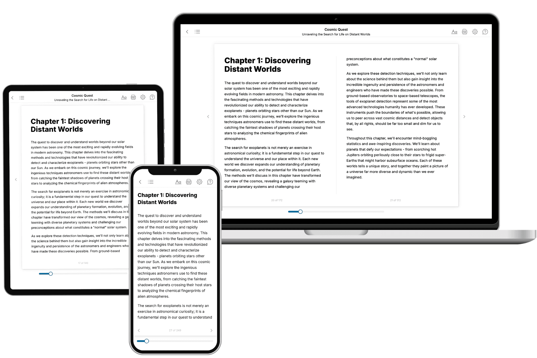
Your book is ready in 10 minutes. Read it online, download as EPUB or PDF, or send to Kindle.

Frequently asked questions
- What is TailoredRead?
TailoredRead creates complete, full-length nonfiction ebooks, written specifically for you. Tell us what you want to learn and why, and TailoredRead writes you a complete ebook on it, with charts, tables, and diagrams throughout. Read it online, on Kindle, or on any e-reader, or download it as a PDF or EPUB. Every book is written fresh the day you order it.
- How is the book tailored to me?
Before anything is written, you answer a few short questions about your goals, your background, and the topics you care about. Your book is then planned around your answers: written at your level, focused on your goals, and covering the topics you chose, instead of the one-size-fits-all book a store sells everyone.
- Will it read like generic AI content?
No. Your book isn't a chat transcript: it's planned chapter by chapter before a single word is written, told in a clear book voice, and explains ideas visually with charts, tables, and diagrams. After writing, every book goes through an editorial pass that polishes chapters so the book reads consistent from start to finish. Judge for yourself: browse thousands of sample books on our Explore Books page.
- How accurate is the content?
Our AI first checks whether your subject needs live research. Niche and fast-moving subjects are researched before writing, and the book plan and chapters are grounded in what it finds. After writing, every book goes through a quality pass that checks its facts and consistency, and researched books list their sources in a Notes section at the back.
- How long is the book?
You choose the length: Comprehensive (250-300 pages), Detailed (150-200 pages), Essential (70-100 pages), or Short (30-50 pages).
- Does the book include visuals?
Yes. Every book includes charts, tables, and diagrams: timelines, checklists, step-by-step guides, decision trees, comparison tables, matrices, and bar charts. A typical book includes dozens of these visual elements.
- Can I read it on Kindle? What formats can I download?
Yes. Every book can be read in our online reader or downloaded as a PDF or EPUB. The EPUB can be opened with Kindle, Apple Books, Kobo, and any e-reader. The Commercial and Author licenses also include an editable Word (DOCX) and Markdown download.
- How much does it cost?
About the price of a regular ebook. The exact price depends on your book's length and complexity, from $2 for the shortest books to $35 for the most comprehensive, and it's shown when you review your book, before you commit to anything. Each book is a one-time purchase, yours to keep, no subscription. Licenses that let you share, teach, or publish your book range from $35.99 to $49.99.
- Can I preview the book before purchasing?
Before you pay, you'll see what your book will cover: the title, a detailed description, the estimated length, and the complete chapter-by-chapter table of contents, so you know what you're getting before you decide. The full text itself is written after you purchase.
- How long does it take to create a book?
About 10 minutes. You can start reading the opening chapters while the rest is still being written.