Semiconductor Manufacturing Fundamentals
From Physics and Chemistry to Fab Operations and Device Integration
Advance your technical mastery of semiconductor manufacturing by building a cohesive understanding of how physics, chemistry, and engineering converge to transform silicon into functional devices.
315 pages16 chaptersSep 1, 2026Semiconductors
About this book
This comprehensive guide connects semiconductor fundamentals—band structure, doping, carrier transport—directly to manufacturing processes and equipment. You'll understand why specific materials, chemicals, and process parameters are used, how individual manufacturing steps integrate into complete technology flows, and how frontend and backend operations work together. Explore CMOS, Bipolar, DMOS, and BCD technologies; master MOSFET and power device physics; and learn how MEMS principles extend semiconductor manufacturing into mechanical domains. Discover the complete 300mm fab ecosystem—from cleanroom infrastructure and wafer handling to metrology, inspection, and final test. Designed for process control engineers, this book provides the technical vocabulary and integrated knowledge needed to communicate effectively with colleagues, understand process interdependencies, and make informed decisions in advanced manufacturing environments.
Table of contents
- IntroductionWhy Semiconductor Manufacturing Matters, How to Use This Book, Building an Integrated Knowledge FrameworkRead below
- Chapter 1: Semiconductor Physics FundamentalsBand Structure and Energy Levels, Doping and Carrier Generation, Carrier Transport and Conductivity, PN Junctions and Depletion Regions
- Chapter 2: Electrical Engineering Fundamentals for SemiconductorsElectric Fields and Potentials in Semiconductors, Current-Voltage Relationships and Device Equations, Capacitance and Charge Storage
- Chapter 3: Semiconductor Materials, Elements, and ChemicalsSilicon Substrates and Crystal Structure, Dopants, Alloys, and Compound Semiconductors, Process Chemicals, Gases, and Precursors, Why Specific Materials Are Used in Manufacturing
- Chapter 4: CMOS, Bipolar, DMOS, and BCD TechnologiesCMOS Technology: Complementary Metal-Oxide-Semiconductor, Bipolar Technology and BJT Devices, DMOS Technology and Power Device Integration, BCD Technology: Integrating Bipolar, CMOS, and DMOS
- Chapter 5: MOSFETs, Power Devices, and Memory TechnologiesMOSFET Structure and Operation, Power Device Physics and High-Voltage Operation, EPROM and Flash Memory Technologies, DRAM, SRAM, and Emerging Memory Architectures
- Chapter 6: MEMS Physics and Bosch MEMS SensorsMEMS Fundamentals: Mechanical and Electrical Integration, The Bosch Process for MEMS Fabrication, MEMS Sensor Operation and Signal Transduction
- Chapter 7: 300mm Semiconductor Fab and Manufacturing Flow300mm Fab Architecture and Layout, Complete Manufacturing Flow: From Wafer to Device, Process Sequences and Technology Integration
- Chapter 8: Lithography and Pattern TransferPhotolithography Principles and Photoresist Chemistry, Photomask Design and Resolution Limits, Lithography Equipment and Process Windows
- Chapter 9: Etching and Plasma ProcessesWet Etching: Chemistry and Selectivity, Dry Etching and Plasma Physics, Etch Equipment, Chambers, and Process Control, Aspect Ratio and Anisotropic Etch Requirements
- Chapter 10: Deposition: PVD, CVD, and EpitaxyPhysical Vapor Deposition and Sputtering, Chemical Vapor Deposition and ALD, Epitaxial Growth and Crystal Quality, Deposition Equipment and Process Parameters
- Chapter 11: Ion Implantation and Thermal ProcessingIon Implantation Physics and Dopant Profiles, Implantation Equipment and Dose Control, Thermal Processing and Diffusion, Annealing and Dopant Activation
- Chapter 12: Wet Chemical Processing, Cleaning, and CMPWet Chemical Processing and Oxide Growth, Wafer Cleaning and Contamination Removal, Chemical Mechanical Planarization and Surface Flattening, Electrochemical Deposition and Copper Interconnects
- Chapter 13: Metrology, Inspection, and Defect DetectionMetrology Techniques and Measurement Systems, Inspection Systems and Defect Detection, Process Control and Feedback Loops
- Chapter 14: Semiconductor Equipment, Automation, and Fab LogisticsProcess Chambers and Equipment Modules, Wafer Handling and Robotic Automation, Fab Logistics and Wafer Flow Management, Equipment Integration and Manufacturing Systems
- Chapter 15: Backend Manufacturing, Assembly, and PackagingFrontend vs. Backend: Process Distinctions, Wafer Sort and Electrical Testing, Die Separation and Packaging Technologies, Final Test and Reliability Assessment
- Chapter 16: Cleanroom, Facilities, and Manufacturing InfrastructureCleanroom Design and Contamination Control, Utilities: Vacuum, Gas, Water, and Power Systems, Chemical Infrastructure and Abatement Systems
- ConclusionIntegrating Physics, Chemistry, and Engineering, Continuing Your Semiconductor Manufacturing Education
- Glossary of Semiconductor Manufacturing Terms and Abbreviations
- Further Reading and Technical Resources
Introduction
A single logic chip that fits on a fingertip passes through hundreds of distinct process steps before it can switch a single transistor. Each step depends on the one before it: a layer deposited too thick throws off the etch that follows, an implant placed a few nanometers off target shifts a threshold voltage that a customer's device will depend on for a decade. For an Advanced Process Control Engineer, this chain of dependency is the actual job. Numbers on a control chart mean little without a working picture of what physically happens inside the chamber that produced them.
A data science background gives strong tools for finding patterns in fab data: drift in a sensor trace, correlation between a recipe parameter and a yield excursion, clustering of failures by tool or chamber. What that background does not automatically supply is the physical vocabulary to explain why the pattern exists. A model can flag that a particular deposition tool produces thinner films on Tuesdays. Only a grasp of the underlying chemistry and equipment mechanics turns that flag into a fix.
This book exists to close that gap. It builds, subsystem by subsystem, the technical foundation that connects a control chart to the physics and chemistry generating it, and connects that physics to the equipment, materials, and fab logistics that make manufacturing possible at scale. Each part of the plan for this book links to the next: physics explains device behavior, device behavior explains why a manufacturing step exists, and manufacturing steps assemble into the complete flow that turns a bare wafer into a packaged, tested part.
Nothing here assumes you already work as a process engineer on the equipment side, and nothing here focuses on machine learning methods themselves. The aim is domain fluency: enough command of semiconductor physics, chemistry, device architecture, and fab operations to read a process specification, follow a discussion with a process engineer or equipment supplier, and reason about a manufacturing problem using the same mental model that the rest of the fab uses.
The chapters that follow move from fundamentals toward the finished factory floor. Physics and electrical engineering come first, then materials, then device families, then the process modules that build those devices, then the equipment and facility systems that host those processes, and finally the backend steps that turn a finished wafer into a shippable product.
Why Semiconductor Manufacturing Matters
Every modern control system, from a smartphone's power management circuit to an industrial robot's sensor array, depends on semiconductor devices manufactured through processes described in later chapters. The industry has recently accelerated its use of computational tools to model these processes before they run on physical equipment, including GPU-accelerated simulation platforms that speed up quantum chemistry and chamber-level modeling by large factors compared to earlier methods[1]. That shift matters for an engineer working in process control because it changes how quickly a proposed recipe change can be evaluated, but it does not change the underlying physics those simulations are built to represent.
Manufacturing a semiconductor device is fundamentally an exercise in controlling matter at scales where quantum mechanical effects, not everyday intuition, govern behavior. A silicon wafer arrives as a nearly perfect crystal. By the time it leaves the fab it carries a three-dimensional structure of transistors, interconnects, and insulators built from hundreds of sequential additions, removals, and transformations of material. Each of those steps has to hit a target measured in nanometers or in parts per million, and each has to do so consistently across a wafer holding billions of devices.
Consider a single transistor's threshold voltage, the voltage at which it switches from off to on. That value depends on the thickness and quality of an oxide layer only a few atoms thick, on the precise concentration of dopant atoms implanted into the silicon beneath it, and on the temperature profile used to activate those dopants afterward. A shift of a few percent in any of those parameters can push a chip out of specification. Manufacturing at this level of precision is not a matter of following a recipe passively. It requires understanding why each parameter is set where it is, so that when a deviation appears, the response addresses the actual physical cause rather than a coincidental correlate.
The stakes of getting this wrong are not abstract. A fab producing chips at high volume can lose enormous value from a single systematic defect that escapes detection for even a few hours, because that defect propagates across every wafer processed on the affected tool during that window. Yield, the fraction of manufactured chips that meet specification, is the single number that most directly reflects how well physics, chemistry, and engineering have been integrated into a working process. Improving yield by even a fraction of a percentage point at scale translates into meaningful cost differences, which is why so much of fab operation centers on metrology, inspection, and statistical process control.
Advanced process control sits at the intersection of all these concerns. It is the discipline of using measured data, drawn from metrology tools and inline sensors, to keep hundreds of interdependent process steps within their required windows despite drift, tool-to-tool variation, and material lot changes. Doing that job well requires more than statistical skill. It requires knowing what a shift in a measured parameter actually implies about the physical state of the wafer, which is why the physics and chemistry chapters in this book precede the equipment and control chapters.
Workforce development in this area has become a visible priority, with university programs expanding their focus on manufacturing and packaging specialization to prepare engineers for roles exactly like the one this book targets[2]. National investment plans in emerging semiconductor manufacturing regions increasingly pair fab construction with talent pipeline development, reflecting an industry-wide recognition that equipment alone does not produce yield[3]. Skilled engineers who understand the full manufacturing stack remain a limiting factor even as automation and simulation tools improve.
None of this technical depth is optional for someone whose job is to keep a fab's processes stable and improving over time. A process control engineer who understands only the statistics of a control chart, without the physics behind the signal, can detect that something changed but cannot reliably diagnose what changed or why. The chapters ahead are built to fill exactly that gap, moving from the physics of carriers in a crystal lattice up through the equipment and facility systems that keep that crystal's transformation under control at industrial scale.
How to Use This Book
The seventeen numbered chapters that follow this introduction are arranged deliberately, building from fundamentals toward finished operations rather than treating each topic as a standalone reference. Chapters 1 through 3 lay the physical and chemical groundwork: semiconductor physics, the electrical engineering relationships built on top of that physics, and the specific materials and chemicals used throughout manufacturing. Chapters 4 through 6 apply that groundwork to device families, from CMOS and bipolar technology through MOSFETs, power devices, memory architectures, and MEMS sensors. Chapters 7 through 16 then walk through the complete fab: its architecture, its process modules in sequence, its equipment and automation systems, its backend assembly steps, and the facility infrastructure that makes all of it possible.
Reading front to back gives the most coherent path through the material, because later chapters routinely assume familiarity with terms and concepts introduced earlier. A discussion of dry etching in Chapter 9, for instance, assumes you already understand the band structure and doping concepts from Chapter 1, since plasma etch selectivity depends partly on the chemical bonding that those physics concepts explain. Skipping ahead is possible and sometimes useful, but expect to backtrack occasionally to a foundational chapter when a term or mechanism feels underexplained.
Each numbered chapter follows a consistent internal pattern. It opens by grounding a concept in a concrete mechanism or example, develops that concept through several subchapters that each isolate one coherent idea, and closes by pointing toward how that idea connects to the next chapter's territory. Subchapters are written to stand somewhat independently as reference material, so once you have read a chapter in full, you can return to a specific subchapter later to refresh a particular concept without rereading the whole chapter.
Terminology is treated with particular care throughout, since imprecise vocabulary is one of the most common sources of miscommunication between process control engineers and process or equipment engineers. Wherever a canonical term exists, such as Critical Dimension, Etch Selectivity, or Dopant Activation, this book uses that exact term consistently rather than switching between synonyms. A glossary near the end of the book collects these terms in one place for quick lookup, and the further reading section beyond it points toward deeper technical resources for anyone who wants to go past the level of detail covered here.
Diagrams and structured elements such as tables, decision trees, and checklists appear where they clarify a comparison or a procedure better than prose alone, but they are used sparingly and only where they add real value. Do not expect one on every page. When one does appear, treat it as a companion to the surrounding paragraphs rather than a replacement for them, since the prose carries the reasoning and the structured element carries the summary.
A practical way to use this book alongside daily work is to treat each chapter as a lens for a specific class of problem encountered on the job. The checklist below suggests how to match a recurring fab situation to the chapter most likely to explain its root cause.
Matching a Fab Situation to a Chapter
- Unexpected threshold voltage shift across a lot: revisit Chapter 5 on MOSFET operation and Chapter 11 on ion implantation
- Film thickness drift on a deposition tool: revisit Chapter 10 on deposition methods and Chapter 13 on metrology
- Etch profile going out of specification: revisit Chapter 9 on etching and plasma processes
- Unexplained particle or defect excursion: revisit Chapter 13 on inspection and Chapter 16 on cleanroom contamination control
- Yield loss traced to a packaging step: revisit Chapter 15 on backend manufacturing and packaging
- Difficulty communicating a process issue with an equipment engineer: revisit Chapter 14 on equipment and automation
Because the reader profile for this book centers on engineers with a strong data science foundation, the material deliberately avoids re-teaching statistical or machine learning concepts that you likely already know well. Where those methods intersect with manufacturing, later chapters on metrology and process control reference the physical quantities being measured and controlled, trusting that the analytical techniques applied to those quantities are already familiar territory. The unfamiliar territory this book targets is the physics, chemistry, and equipment side of the equation.
Reading actively rather than passively will pay off more here than in most technical books. Whenever a concept connects to something you already handle in a control system or a dataset, such as a sensor trace correlated with a chamber pressure setpoint, pause and work out explicitly why the physical mechanism produces that correlation. That habit of connecting abstract mechanism to concrete signal is exactly the skill this book is designed to build, and it strengthens fastest through deliberate practice while reading rather than through passive absorption of the text.
Finally, treat the numbered chapters as a reference to revisit over time rather than a single pass to complete once. Semiconductor manufacturing knowledge compounds: a concept that feels abstract on first reading, such as the drift-diffusion behavior underlying carrier transport, often becomes concrete only once you have seen it show up in a specific tool's behavior or a specific yield investigation. Returning to the relevant chapter after encountering that real situation will deepen the understanding far more than rereading it in isolation would.
Building an Integrated Knowledge Framework
The central argument of this book is that semiconductor manufacturing cannot be understood as a collection of separate disciplines stacked side by side. Physics determines what a device can do, chemistry determines what materials and reactions can build that device, and engineering determines how those materials and reactions are delivered reliably at the scale of a modern fab. Treating these as three independent subjects, learned in isolation, leaves gaps exactly where the real technical problems live: at the interfaces between them.
A useful way to see this integration is to trace one physical quantity through the entire book's structure. Take dopant concentration, the density of impurity atoms deliberately introduced into silicon. Chapter 1 explains how those dopant atoms alter the material's band structure and generate free carriers. Chapter 5 explains how the resulting carrier density sets a MOSFET's threshold voltage. Chapter 11 explains how ion implantation physically introduces those dopants and how annealing activates them. Chapter 13 explains how metrology tools verify that the resulting dopant profile matches its target. A single physical quantity, followed through four chapters, links quantum mechanics to a measurement report on a fab floor.
This same pattern repeats across nearly every topic in the book. A gate oxide's thickness connects capacitance behavior from Chapter 2 to thermal oxidation chemistry from Chapter 12 to the process window constraints discussed in Chapter 8's coverage of lithography and Chapter 13's coverage of metrology. A copper interconnect's resistance connects electrical engineering fundamentals to electrochemical deposition chemistry to chemical mechanical planarization to defect inspection. Recognizing these threads as you read is more valuable than memorizing any single chapter's content in isolation, because real manufacturing problems almost always sit at the junction of two or more of these threads rather than cleanly inside one.
Physics-informed approaches to modeling manufacturing processes have gained attention recently as a way to keep computational models grounded in real physical constraints rather than relying purely on data-driven pattern matching[4]. This trend mirrors exactly the argument made throughout this book: a model, whether it lives in software or in an engineer's head, becomes more reliable when it is anchored to the physical mechanisms actually producing the observed behavior. A control engineer who understands why a process behaves as it does can evaluate a proposed model or a proposed fix far more critically than one who only sees inputs and outputs.
Building this integrated framework also means getting comfortable moving between very different scales of description within a single conversation. A discussion of yield loss might start at the scale of a wafer lot, move down to a single tool's chamber conditions, move further down to the atomic-scale chemistry of a plasma reaction, and then move back up to the economic consequence of the defect at the lot level. Semiconductor manufacturing routinely demands this kind of scale-shifting, and the chapters in this book are organized specifically to build fluency in moving between them without losing the thread connecting one scale to the next.
One further habit worth building deliberately is translating between the vocabulary of different technical specialties. A process engineer might describe a problem in terms of a recipe parameter, an equipment engineer in terms of a chamber component, and a device physicist in terms of a carrier concentration, when all three are describing the same underlying event from different vantage points. Part of what this book provides is the shared vocabulary that lets a process control engineer participate credibly in all three of those conversations, rather than depending on translation from someone else.
By the time you reach the conclusion of this book, the goal is not to have memorized every process recipe or every equipment specification discussed along the way. Recipes and specifications change with every new technology node and every new tool generation, and no book can keep pace with that rate of change. The lasting value instead comes from the framework itself, the ability to reason from first principles about why a given step exists, what physical outcome it is meant to produce, and how a deviation from that outcome will ripple through every step that follows. That framework, once built, transfers to whatever specific technology, tool, or node you encounter next in an actual fab.
Notes
Introduction
- 1. Applied Materials, "Applied Materials and NVIDIA Collaboration Accelerates Semiconductor Process Simulation," Applied Materials, 2026
- 2. Purdue University, "Purdue Semiconductor Degrees Program Expands to Meet Workforce Demand," Purdue University, 2026
- 3. India Semiconductor Mission, "India Semiconductor Roadmap Emphasizes Talent Development," India Semiconductor Mission, 2026
- 4. Semiconductor Research Corporation, "Physics-Informed Generative Models for Semiconductor Manufacturing Research Agenda," Semiconductor Research Corporation, 2026
This is the end of the free sample. The full book has 16 chapters.
Want this book written for you?
Tell us your goals and background, and get your own version of this book, tailored by AI to you.


Benefits of AI-tailored books
- Read one book, not ten:
- all the Semiconductors knowledge you need, gathered into a single book.
- Save days of learning:
- tell us your goals, choose your topics, and the whole book is built around them.
- Learn effortlessly:
- Semiconductors book written for your specific background and expertise.
- Understand at a glance:
- includes charts, tables, timelines, checklists, decision trees, and more.
- Stay current:
- written the day you order it, not years ago.
- Trust what you read:
- every book is checked for accuracy, with real research when your subject needs it.
Create your unique book in 3 steps
- 1. Select your focus
Select the focus of your Semiconductors book and share your background
- 2. Personalize your book
Specify your goals and choose sub-topics to include
- 3. Get your tailored book
Your book is ready in 10 minutes. Read it online, download as EPUB or PDF, or send to Kindle.


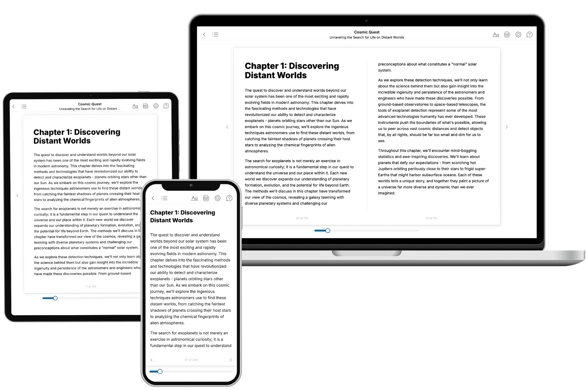
Frequently asked questions
- What is TailoredRead?
TailoredRead creates complete, full-length nonfiction ebooks, written specifically for you. Tell us what you want to learn and why, and TailoredRead writes you a complete ebook on it, with charts, tables, and diagrams throughout. Read it online, on Kindle, or on any e-reader, or download it as a PDF or EPUB. Every book is written fresh the day you order it.
- How is the book tailored to me?
Before anything is written, you answer a few short questions about your goals, your background, and the topics you care about. Your book is then planned around your answers: written at your level, focused on your goals, and covering the topics you chose, instead of the one-size-fits-all book a store sells everyone.
- Will it read like generic AI content?
No. Your book isn't a chat transcript: it's planned chapter by chapter before a single word is written, told in a clear book voice, and explains ideas visually with charts, tables, and diagrams. After writing, every book goes through an editorial pass that polishes chapters so the book reads consistent from start to finish. Judge for yourself: browse thousands of sample books on our Explore Books page.
- How accurate is the content?
Our AI first checks whether your subject needs live research. Niche and fast-moving subjects are researched before writing, and the book plan and chapters are grounded in what it finds. After writing, every book goes through a quality pass that checks its facts and consistency, and researched books list their sources in a Notes section at the back.
- How long is the book?
You choose the length: Comprehensive (250-300 pages), Detailed (150-200 pages), Essential (70-100 pages), or Short (30-50 pages).
- Does the book include visuals?
Yes. Every book includes charts, tables, and diagrams: timelines, checklists, step-by-step guides, decision trees, comparison tables, matrices, and bar charts. A typical book includes dozens of these visual elements.
- Can I read it on Kindle? What formats can I download?
Yes. Every book can be read in our online reader or downloaded as a PDF or EPUB. The EPUB can be opened with Kindle, Apple Books, Kobo, and any e-reader. The Commercial and Author licenses also include an editable Word (DOCX) and Markdown download.
- How much does it cost?
About the price of a regular ebook. The exact price depends on your book's length and complexity, from $2 for the shortest books to $35 for the most comprehensive, and it's shown when you review your book, before you commit to anything. Each book is a one-time purchase, yours to keep, no subscription. Licenses that let you share, teach, or publish your book range from $35.99 to $49.99.
- Can I preview the book before purchasing?
Before you pay, you'll see what your book will cover: the title, a detailed description, the estimated length, and the complete chapter-by-chapter table of contents, so you know what you're getting before you decide. The full text itself is written after you purchase.
- How long does it take to create a book?
About 10 minutes. You can start reading the opening chapters while the rest is still being written.