Wafer Level Packaging Essentials
Master the Fundamentals of Modern Semiconductor Packaging Technology
Discover how wafer-level packaging is revolutionizing semiconductor manufacturing and enabling the next generation of compact, high-performance devices.
207 pages9 chaptersJan 16, 2026Electronics Engineering
About this book
This comprehensive guide walks you through the complete landscape of WLP technologies, from fundamental concepts to advanced implementation strategies. You'll explore the physics and engineering principles behind flip-chip bonding, fan-out wafer-level packaging, and 3D stacking techniques. Learn how to navigate the critical decisions around material selection, thermal management, and reliability testing. Whether you're designing your first WLP solution or optimizing existing processes, this book provides the practical knowledge and strategic insights needed to succeed in today's competitive semiconductor industry. Gain clarity on cost-benefit analyses, manufacturing challenges, and quality assurance practices that separate successful implementations from costly failures.
Table of contents
- IntroductionWhy Wafer-Level Packaging Matters Today, The Evolution of Semiconductor Packaging, Your Roadmap Through This BookRead below
- Chapter 1: Fundamentals of Wafer-Level PackagingWhat Is Wafer-Level Packaging?, Advantages and Limitations of WLP, WLP vs. Traditional Packaging Methods
- Chapter 2: Core WLP TechnologiesFlip-Chip Bonding: Principles and Process, Fan-Out Wafer-Level Packaging (FOWLP), 3D Stacking and Through-Silicon Vias (TSVs), Emerging WLP Technologies and Innovations
- Chapter 3: Design Principles for WLPCritical Design Considerations, Design for Manufacturability (DFM) Integration, Electrical Design and Signal Integrity
- Chapter 4: Thermal Management in WLPUnderstanding Thermal Challenges, Heat Dissipation Strategies and Materials, Thermal Modeling and Simulation
- Chapter 5: Materials and Interconnection TechnologiesSubstrate Materials and Selection, Bonding Materials and Adhesives, Interconnect Options: Solder, Copper, and Beyond
- Chapter 6: Manufacturing Processes and Yield OptimizationComplete WLP Process Flow, Key Factors Affecting Yield, Strategies for Yield Improvement
- Chapter 7: Reliability and Quality AssuranceReliability Testing Standards and Methods, Common Failure Modes and Prevention, Quality Metrics and Assurance Practices
- Chapter 8: Cost Analysis and Economic ConsiderationsUnderstanding WLP Cost Drivers, Cost-Benefit Analysis for WLP Selection, Scaling Economics and Volume Production
- Chapter 9: Real-World Applications and Case StudiesMobile and Consumer Electronics Applications, High-Performance Computing and Data Centers, Automotive and IoT Applications
- ConclusionKey Takeaways and Best Practices, The Future of Wafer-Level Packaging
- Glossary of Terms
- Further Reading and Resources
Introduction
The semiconductor industry stands at a critical juncture where traditional packaging approaches can no longer keep pace with the relentless demands for smaller, faster, and more power-efficient devices. Every smartphone, wearable device, and high-performance computing system you encounter today relies on packaging technologies that were unimaginable just two decades ago. Wafer-level packaging has emerged as the cornerstone solution to these challenges, fundamentally transforming how semiconductor devices transition from silicon wafers to functional products. This shift represents more than incremental improvement—it's a complete reimagining of the relationship between chip design, manufacturing, and final product performance.
For electronics professionals and VLSI engineers, understanding wafer-level packaging is no longer optional—it's essential for staying relevant in an industry that evolves at breakneck speed. The decisions you make about packaging architecture directly impact product performance, manufacturing costs, time-to-market, and competitive positioning. Whether you're designing application processors for mobile devices, developing high-bandwidth memory solutions, or creating sensor systems for automotive applications, WLP technologies will shape your design constraints and opportunities. The knowledge gap between those who understand these technologies and those who don't continues to widen, creating both challenges and opportunities for professionals willing to invest in deepening their expertise.
This book serves as your comprehensive guide through the complex landscape of wafer-level packaging technologies. Unlike purely theoretical treatments or narrowly focused technical papers, this resource bridges the gap between fundamental principles and practical implementation. You'll gain insights into the physics and engineering that make WLP possible, the manufacturing realities that constrain design choices, and the economic factors that determine commercial viability. Each chapter builds systematically on previous concepts while remaining accessible to readers with intermediate semiconductor knowledge. By the time you complete this journey, you'll possess the analytical frameworks and practical knowledge needed to make informed decisions about WLP technology selection, design optimization, and manufacturing strategy.
Why Wafer-Level Packaging Matters Today
The explosive growth of mobile computing, Internet of Things devices, and artificial intelligence applications has created unprecedented demands on semiconductor packaging. Modern smartphones contain more computing power than supercomputers from the 1990s, yet they fit in your pocket and operate for days on a single battery charge. This remarkable achievement stems largely from advances in wafer-level packaging that enable higher integration density, shorter interconnect paths, and superior thermal management. Traditional packaging methods simply cannot deliver the combination of small form factor, high performance, and acceptable cost that today's applications demand. WLP technologies address these requirements by performing packaging operations at the wafer level before individual die separation, fundamentally changing the economics and capabilities of semiconductor manufacturing.
Consider the practical implications for product development timelines and competitive advantage. When Apple introduced the iPhone in 2007, it relied heavily on advanced packaging technologies to achieve its revolutionary thin profile and performance characteristics. Companies that understood and could implement these packaging solutions gained significant market advantages, while those relying on conventional approaches found themselves unable to compete effectively. This pattern has repeated across numerous product categories, from wearable fitness trackers to high-performance graphics processors. The ability to leverage WLP technologies directly translates to product differentiation, faster time-to-market, and improved profit margins. Organizations that treat packaging as an afterthought rather than a core competency increasingly find themselves at a competitive disadvantage.
The technical advantages of wafer-level packaging extend across multiple critical dimensions that directly impact product success:
- Reduced form factor: WLP eliminates the need for traditional package substrates and wire bonds, reducing overall package thickness by 50-80% compared to conventional approaches
- Improved electrical performance: Shorter interconnect paths reduce parasitic inductance and capacitance, enabling higher operating frequencies and lower power consumption
- Enhanced thermal management: Direct heat dissipation paths from die to external environment improve thermal performance by 30-40% in typical applications
- Superior reliability: Elimination of wire bonds removes a common failure mechanism, while wafer-level testing catches defects before final assembly
- Cost efficiency at scale: Parallel processing of hundreds or thousands of devices simultaneously reduces per-unit packaging costs in high-volume production
Beyond these technical benefits, WLP enables entirely new product categories and applications that were previously impractical or impossible. Ultra-thin smart cards with embedded processors, implantable medical devices with sophisticated sensing capabilities, and millimeter-scale IoT sensors all depend on WLP technologies to achieve their size and performance targets. The technology has become particularly critical in applications requiring heterogeneous integration, where different semiconductor technologies must be combined in a single package. For example, combining radio-frequency circuits, digital logic, and MEMS sensors in a compact module for wireless sensor networks would be prohibitively expensive or technically infeasible without advanced WLP approaches. This enabling characteristic makes WLP knowledge essential for anyone involved in next-generation product development.
The market dynamics surrounding WLP further underscore its importance to your professional development. The global wafer-level packaging market exceeded $15 billion in 2023 and continues growing at double-digit annual rates, driven by insatiable demand for mobile devices, automotive electronics, and data center infrastructure[1]. Major semiconductor manufacturers have invested billions of dollars in WLP production capacity, recognizing it as a strategic differentiator rather than a commodity service. Companies like TSMC, Samsung, and Intel now compete as much on packaging capabilities as on transistor technology. This shift creates expanding career opportunities for engineers who understand both the technical and business aspects of WLP, while simultaneously raising the bar for what constitutes adequate knowledge in semiconductor engineering roles.
Environmental and sustainability considerations add another dimension to WLP's growing importance. Traditional packaging approaches generate substantial material waste through substrate fabrication, wire bonding processes, and individual package assembly. WLP technologies reduce material consumption by eliminating unnecessary package components and enabling more efficient use of wafer real estate. The reduction in package size also decreases shipping volumes and associated carbon emissions across global supply chains. As semiconductor companies face increasing pressure to meet sustainability targets and reduce environmental impact, WLP offers tangible pathways to improvement. Understanding these environmental benefits and trade-offs will become increasingly important as regulatory requirements and customer expectations evolve in coming years.
Perhaps most critically, WLP represents a fundamental shift in how semiconductor professionals must think about product development. The traditional sequential approach—where chip design, packaging, and system integration occur as separate, largely independent activities—no longer works effectively with advanced WLP technologies. Instead, successful implementation requires concurrent engineering where packaging considerations influence chip architecture from the earliest design stages. This paradigm shift demands that VLSI engineers develop broader knowledge spanning multiple disciplines, from materials science to thermal physics to manufacturing economics. The professionals who thrive in this environment are those who can bridge traditional boundaries and think holistically about the complete product development cycle.
The Evolution of Semiconductor Packaging
Understanding where wafer-level packaging fits in the broader history of semiconductor packaging provides essential context for appreciating its significance and predicting future directions. The first integrated circuits in the 1960s used simple dual in-line packages (DIPs) with through-hole pins that could be easily inserted into printed circuit boards. These packages were large, expensive, and limited in I/O count, but they matched the capabilities and requirements of early semiconductor devices. As transistor counts increased and operating frequencies rose through the 1970s and 1980s, packaging evolved to surface-mount technologies like quad flat packages (QFPs) and plastic leaded chip carriers (PLCCs). These advances reduced package size and improved electrical performance, but they maintained the fundamental approach of assembling individual die into discrete packages after wafer fabrication and testing.
The 1990s brought the first significant departures from traditional packaging paradigms with the introduction of ball grid array (BGA) packages and flip-chip bonding techniques. BGAs replaced peripheral leads with an array of solder balls across the package bottom, dramatically increasing available I/O count and improving thermal performance. Flip-chip technology, originally developed by IBM in the 1960s but not widely commercialized until decades later, eliminated wire bonds by directly connecting the active die surface to the package substrate through solder bumps. These innovations addressed the growing performance demands of microprocessors and graphics chips, but they still involved packaging individual die after singulation. The industry had not yet made the conceptual leap to performing packaging operations at the wafer level before separating individual devices.
The true wafer-level packaging revolution began in the late 1990s and early 2000s, driven primarily by the mobile device industry's insatiable appetite for smaller, thinner components. Early WLP implementations focused on relatively simple devices like MEMS sensors and low-pin-count logic chips, where the technology could deliver immediate size and cost benefits. These pioneering applications demonstrated the viability of the approach and drove development of the specialized equipment and processes required for volume production. Companies like Shellcase and APTOS (later acquired by Amkor and Nanium respectively) commercialized the first fan-in WLP technologies, proving that wafer-level redistribution and bumping could achieve acceptable yields and reliability. The success of these early implementations created momentum for expanding WLP to more complex devices and applications.
The evolution of WLP technologies has followed several distinct trajectories, each addressing different market needs and technical challenges:
- Fan-in WLP (2000-2005): Initial implementations limited to die-size packages with redistribution layers connecting die pads to peripheral solder balls
- Fan-out WLP (2005-2010): Introduction of reconstituted wafer approaches enabling packages larger than the original die, supporting higher I/O counts and improved thermal performance
- 3D integration (2010-2015): Development of through-silicon via (TSV) technology enabling vertical stacking of multiple die with high-bandwidth interconnections
- Chiplet architectures (2015-present): Advanced fan-out and 3D technologies enabling heterogeneous integration of die from different process nodes and technologies
- Hybrid bonding (2020-present): Emerging copper-to-copper direct bonding techniques eliminating solder bumps and enabling ultra-fine-pitch interconnections
Each evolutionary step addressed specific limitations of previous approaches while introducing new capabilities and challenges. Fan-out WLP overcame the I/O limitations of fan-in packages but required new reconstitution processes and equipment. TSV-based 3D integration enabled unprecedented bandwidth between stacked die but introduced thermal management challenges and yield complexities. Chiplet architectures promise to extend Moore's Law economics by mixing and matching optimized die, but they demand new design methodologies and standardized interfaces. This pattern of innovation creating both opportunities and challenges continues to drive the field forward, ensuring that WLP remains a dynamic and evolving technology landscape rather than a mature, stable domain.
The competitive dynamics between different packaging approaches have shaped industry structure and investment patterns in profound ways. When TSMC introduced its Integrated Fan-Out (InFO) technology for Apple's A10 processor in 2016, it demonstrated that leading-edge logic devices could successfully transition to advanced WLP, not just simple peripheral chips. This milestone triggered massive investments by other foundries and outsourced assembly and test (OSAT) providers to develop competing fan-out capabilities. Samsung responded with its Fan-Out Panel Level Packaging (FOPLP) approach, while Intel invested heavily in its Embedded Multi-die Interconnect Bridge (EMIB) technology. These competitive pressures accelerated innovation and drove rapid improvements in process capabilities, yield, and cost-effectiveness across the industry.
Looking at this evolution from a systems perspective reveals how packaging advances have enabled broader architectural innovations in semiconductor products. The transition from single-die packages to multi-chip modules and now to advanced chiplet architectures represents a fundamental shift in how complex systems are designed and manufactured. Instead of attempting to integrate all functionality on a single monolithic die—which becomes increasingly expensive and risky at advanced process nodes—designers can now partition systems into optimized chiplets connected through advanced packaging. This approach allows mixing different semiconductor technologies (logic, memory, analog, photonics) that would be impossible or impractical to integrate on a single die. The packaging technology thus becomes an enabler of system architecture innovation, not merely a necessary step in the manufacturing process.
The historical trajectory of packaging evolution also illuminates important lessons about technology adoption and industry transformation. New packaging technologies typically require 5-10 years from initial development to widespread commercial adoption, as equipment suppliers, materials vendors, and manufacturing organizations build the necessary ecosystem. Early implementations often target niche applications where the technology's advantages clearly outweigh its limitations and higher costs. As volumes increase and learning curves progress, costs decline and capabilities improve, enabling expansion into broader markets. Understanding this adoption pattern helps you anticipate which emerging WLP technologies are likely to achieve commercial significance and which may remain specialized solutions for specific applications. This perspective proves invaluable when making strategic decisions about technology investments and product roadmaps.
Your Roadmap Through This Book
This book is structured to build your understanding systematically, starting with fundamental concepts and progressing through increasingly sophisticated topics and applications. Each chapter focuses on a specific aspect of wafer-level packaging while maintaining connections to the broader context of semiconductor manufacturing and product development. The organization reflects how WLP knowledge is actually applied in professional practice—beginning with technology selection and design principles, moving through implementation details and manufacturing considerations, and concluding with real-world applications and economic analysis. This structure allows you to develop both breadth and depth of understanding, whether you're reading cover-to-cover or focusing on specific chapters most relevant to your immediate needs.
Chapter 1 establishes the foundational knowledge you'll need throughout the rest of the book. You'll explore what distinguishes wafer-level packaging from traditional approaches, examining the core principles that make WLP possible and practical. The chapter provides a balanced assessment of WLP advantages and limitations, helping you understand when these technologies make sense and when conventional packaging might be more appropriate. You'll also gain clarity on the key differences between WLP and traditional packaging methods across multiple dimensions—technical performance, manufacturing processes, cost structures, and design considerations. This foundation ensures you can make informed comparisons and trade-offs as you encounter more advanced topics in later chapters.
Chapter 2 dives into the major WLP technology families that dominate current production and development efforts. You'll examine flip-chip bonding in detail, understanding the physics of solder bump formation, reflow processes, and underfill application. The chapter then explores fan-out wafer-level packaging, including both chip-first and chip-last process flows and their respective advantages. Three-dimensional integration through TSVs receives thorough treatment, covering via formation, filling, and the unique challenges of stacking multiple die. The chapter concludes with a survey of emerging technologies like hybrid bonding and panel-level packaging that may shape the industry's future. By the end of this chapter, you'll understand the technical distinctions between major WLP approaches and the applications where each excels.
The design-focused content in Chapter 3 addresses the critical early-stage decisions that determine WLP project success or failure. You'll learn how to evaluate design trade-offs between electrical performance, thermal management, mechanical reliability, and manufacturing cost. The chapter emphasizes design for manufacturability principles specific to WLP, including redistribution layer design rules, bump pitch selection, and die placement considerations for fan-out packages. Electrical design topics cover signal integrity challenges unique to WLP structures, power distribution network design, and electromagnetic interference mitigation. This chapter provides the analytical frameworks you need to translate product requirements into effective WLP design specifications.
Chapter 4 tackles thermal management, one of the three critical pillars of WLP success alongside electrical performance and mechanical reliability. The chapter begins by quantifying the thermal challenges in modern high-power devices and explaining why traditional packaging approaches often fall short. You'll explore various heat dissipation strategies, from simple thermal interface materials to sophisticated integrated heat spreaders and active cooling solutions. Material selection receives detailed attention, with specific thermal conductivity data and application guidelines for common options. The chapter also covers thermal modeling and simulation techniques, providing practical guidance on using computational tools to predict and optimize thermal performance before committing to expensive prototypes.
Materials and interconnection technologies form the subject of Chapter 5, examining the physical components that make WLP structures possible:
- Substrate materials: Silicon, glass, and organic substrates with their respective advantages, limitations, and typical applications
- Redistribution layer materials: Dielectric polymers and metals used to create routing layers, including process compatibility and reliability considerations
- Bonding materials: Solder alloys, conductive adhesives, and emerging direct bonding approaches with detailed property comparisons
- Underfill and molding compounds: Materials that provide mechanical support and environmental protection with their selection criteria
- Thermal interface materials: Options for managing heat transfer between die and external heat sinks or spreaders
Manufacturing processes and yield optimization receive comprehensive treatment in Chapter 6, bridging the gap between design intent and production reality. You'll follow the complete WLP process flow from wafer preparation through final testing and singulation, understanding the purpose and critical parameters of each step. The chapter identifies key factors affecting yield, including defect sources, process variations, and handling damage. Practical yield improvement strategies are presented with specific examples and quantified benefits. This chapter proves particularly valuable for readers involved in transitioning WLP designs from development to volume production, where yield directly impacts profitability and competitiveness.
Reliability and quality assurance topics in Chapter 7 address how to ensure WLP products meet their intended lifetime and performance requirements. You'll learn about industry-standard reliability testing methods including temperature cycling, high-temperature storage, and accelerated moisture testing. Common failure modes specific to WLP structures receive detailed analysis, along with design and process modifications that prevent or mitigate these failures. The chapter also covers quality metrics and statistical process control approaches appropriate for WLP manufacturing. Understanding these reliability considerations enables you to design robust products and establish appropriate qualification programs for new WLP implementations.
Chapter 8 provides the economic analysis frameworks essential for making sound business decisions about WLP technology adoption. You'll learn to identify and quantify the major cost drivers in WLP manufacturing, from wafer processing to materials to testing and yield losses. The chapter presents structured approaches to cost-benefit analysis that account for both direct manufacturing costs and indirect factors like time-to-market and product differentiation. Scaling economics receive particular attention, as the cost structure of WLP changes dramatically between prototype, pilot production, and high-volume manufacturing. This chapter equips you to participate effectively in technology selection discussions and business case development for WLP projects.
The book concludes with Chapter 9, which brings together concepts from previous chapters through detailed examination of real-world applications. You'll explore how WLP technologies enable specific product categories in mobile devices, high-performance computing, automotive systems, and IoT applications. Each application area receives treatment of its unique requirements, the WLP approaches that best address those requirements, and specific examples of successful implementations. These case studies illustrate how the technical, manufacturing, and economic considerations discussed in earlier chapters come together in actual product development scenarios. The chapter helps you translate abstract knowledge into practical insights applicable to your own projects and applications.
Throughout the book, you'll encounter specific examples, quantitative data, and practical guidelines rather than purely theoretical discussions. Each major concept includes implementation details, common pitfalls to avoid, and troubleshooting approaches for when things don't go as planned. The content draws on both published research and industry experience to provide balanced perspectives on what works, what doesn't, and why. Whether you're designing your first WLP product, optimizing an existing manufacturing process, or evaluating technology options for a new application, you'll find actionable information to support your decision-making and implementation efforts. The goal is not merely to inform but to equip you with knowledge you can immediately apply to real engineering challenges in your professional work.
Notes
Introduction
- 1. Yole Développement, Advanced Packaging Market Monitor Report, 2023
This is the end of the free sample. The full book has 9 chapters.
Want this book written for you?
Tell us your goals and background, and get your own version of this book, tailored by AI to you.


Benefits of AI-tailored books
- Read one book, not ten:
- all the Electronics Engineering knowledge you need, gathered into a single book.
- Save days of learning:
- tell us your goals, choose your topics, and the whole book is built around them.
- Learn effortlessly:
- Electronics Engineering book written for your specific background and expertise.
- Understand at a glance:
- includes charts, tables, timelines, checklists, decision trees, and more.
- Stay current:
- written the day you order it, not years ago.
- Trust what you read:
- every book is checked for accuracy, with real research when your subject needs it.
Create your unique book in 3 steps
- 1. Select your focus
Select the focus of your Electronics Engineering book and share your background
- 2. Personalize your book
Specify your goals and choose sub-topics to include
- 3. Get your tailored book
Your book is ready in 10 minutes. Read it online, download as EPUB or PDF, or send to Kindle.

Frequently asked questions
- What is TailoredRead?
TailoredRead creates complete, full-length nonfiction ebooks, written specifically for you. Tell us what you want to learn and why, and TailoredRead writes you a complete ebook on it, with charts, tables, and diagrams throughout. Read it online, on Kindle, or on any e-reader, or download it as a PDF or EPUB. Every book is written fresh the day you order it.
- How is the book tailored to me?
Before anything is written, you answer a few short questions about your goals, your background, and the topics you care about. Your book is then planned around your answers: written at your level, focused on your goals, and covering the topics you chose, instead of the one-size-fits-all book a store sells everyone.
- Will it read like generic AI content?
No. Your book isn't a chat transcript: it's planned chapter by chapter before a single word is written, told in a clear book voice, and explains ideas visually with charts, tables, and diagrams. After writing, every book goes through an editorial pass that polishes chapters so the book reads consistent from start to finish. Judge for yourself: browse thousands of sample books on our Explore Books page.
- How accurate is the content?
Our AI first checks whether your subject needs live research. Niche and fast-moving subjects are researched before writing, and the book plan and chapters are grounded in what it finds. After writing, every book goes through a quality pass that checks its facts and consistency, and researched books list their sources in a Notes section at the back.
- How long is the book?
You choose the length: Comprehensive (250-300 pages), Detailed (150-200 pages), Essential (70-100 pages), or Short (30-50 pages).
- Does the book include visuals?
Yes. Every book includes charts, tables, and diagrams: timelines, checklists, step-by-step guides, decision trees, comparison tables, matrices, and bar charts. A typical book includes dozens of these visual elements.
- Can I read it on Kindle? What formats can I download?
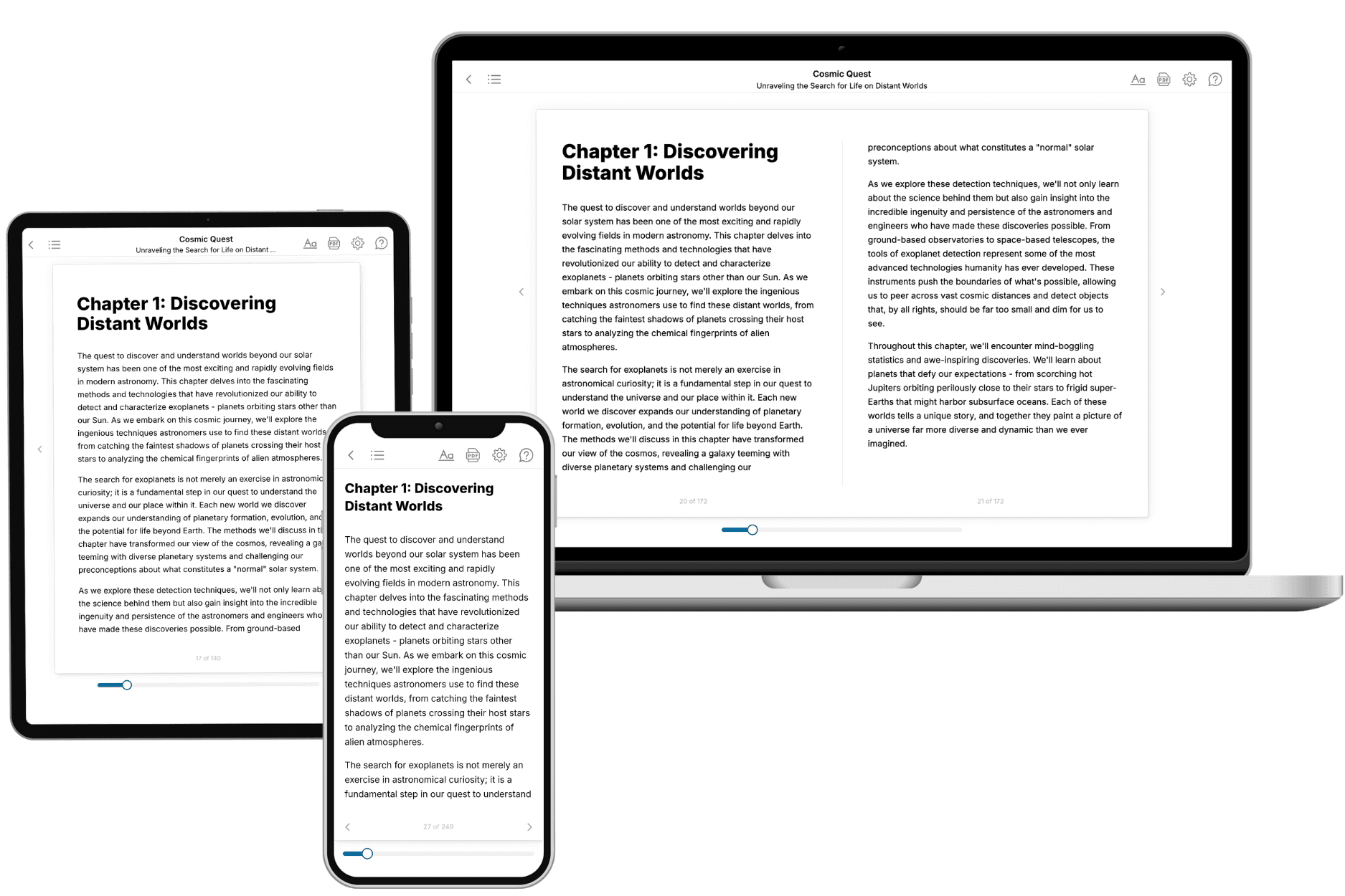
Yes. Every book can be read in our online reader or downloaded as a PDF or EPUB. The EPUB can be opened with Kindle, Apple Books, Kobo, and any e-reader. The Commercial and Author licenses also include an editable Word (DOCX) and Markdown download.
- How much does it cost?
About the price of a regular ebook. The exact price depends on your book's length and complexity, from $2 for the shortest books to $35 for the most comprehensive, and it's shown when you review your book, before you commit to anything. Each book is a one-time purchase, yours to keep, no subscription. Licenses that let you share, teach, or publish your book range from $35.99 to $49.99.
- Can I preview the book before purchasing?
Before you pay, you'll see what your book will cover: the title, a detailed description, the estimated length, and the complete chapter-by-chapter table of contents, so you know what you're getting before you decide. The full text itself is written after you purchase.
- How long does it take to create a book?
About 10 minutes. You can start reading the opening chapters while the rest is still being written.