Advanced VLSI Design
Mastering Secure and High-Performance Chip Architecture for Next-Generation Communications
In the rapidly evolving world of ultra-high-speed communications, the challenge of designing secure and efficient chips has never been more daunting.
315 pages16 chaptersJul 13, 2025Electronics
About this book
As a Principal Architect, you face the complex task of integrating cutting-edge VLSI techniques with robust cryptographic solutions. This book is your comprehensive guide to conquering these challenges. "Advanced VLSI Design" delves deep into the intricacies of modern chip architecture, offering you practical insights into overcoming CMOS scaling limitations, harnessing the power of 3D IC integration, and implementing state-of-the-art FinFET technology. You'll explore innovative approaches to low-power design and high-speed SerDes, crucial for next-generation communication systems. This book doesn't just stop at performance; it equips you with the knowledge to build security from the ground up. From hardware Trojan detection to side-channel analysis resistance, you'll learn how to create chips that are not only fast but also fortified against modern security threats. Dive into advanced topics like quantum-dot cellular automata and EUV lithography, positioning yourself at the forefront of VLSI innovation.
Table of contents
- IntroductionVLSI: Past, Present, and Future, Security Challenges in Modern Chip Design, Book Structure and How to Use It, Current Industry Trends and Future ProjectionsRead below
- Chapter 1: CMOS Scaling Challenges and SolutionsUnderstanding CMOS Scaling Limits, Beyond Moore's Law: New Paradigms, Advanced Materials for CMOS Scaling, Design Techniques to Mitigate Scaling Issues
- Chapter 2: 3D IC Integration TechniquesBenefits and Challenges of 3D Integration, Through-Silicon Via (TSV) Technology, Thermal Management in 3D ICs, Testing and Yield Improvement for 3D ICs
- Chapter 3: FinFET Technology and Design ConsiderationsFinFET Basics and Advantages, Modeling and Simulation of FinFET Devices, Circuit Design with FinFET Technology, Overcoming FinFET Design Challenges
- Chapter 4: Low-Power Design StrategiesPower Analysis and Estimation Techniques, Dynamic Power Reduction Methods, Leakage Power Minimization, Power Gating Techniques, Dynamic Voltage and Frequency Scaling
- Chapter 5: High-Speed SerDes DesignSerDes Architecture Overview, Transmitter Design Techniques, Receiver Design and Equalization, Clocking and Synchronization in SerDes
- Chapter 6: On-Chip Interconnects and Network-on-ChipInterconnect Challenges in Modern VLSI, Network-on-Chip Architectures, Routing Algorithms for NoC, Quality of Service in NoC Design
- Chapter 7: Clock Distribution NetworksClock Tree Synthesis Techniques, Managing Clock Skew and Jitter, Resonant Clocking for Power Efficiency, Adaptive Clocking Strategies
- Chapter 8: Asynchronous Circuit DesignAdvantages of Asynchronous Design, Handshaking Protocols and Circuit Templates, Asynchronous Pipeline Design, Tools and Methodologies for Asynchronous Design
- Chapter 9: Radiation Hardening TechniquesUnderstanding Radiation Effects on ICs, Circuit-Level Radiation Hardening, Layout Techniques for Radiation Tolerance, Error Detection and Correction Strategies
- Chapter 10: Thermal Management in VLSI SystemsThermal Modeling and Analysis, Heat Dissipation Techniques, Dynamic Thermal Management, Thermal Challenges in 3D ICs
- Chapter 11: Emerging VLSI TechnologiesQuantum-Dot Cellular Automata, EUV Lithography Advancements, Neuromorphic Computing Architectures, Photonic Integrated Circuits
- Chapter 12: Hardware Security in VLSI DesignHardware Trojan Detection and Prevention, Side-Channel Analysis and Countermeasures, Physical Unclonable Function (PUF) Design, Post-Quantum Cryptography Hardware
- Chapter 13: Cryptographic Hardware ImplementationAES Hardware Design Optimization, Secure Boot Mechanisms, Trusted Execution Environments, Differential Power Analysis Countermeasures
- Chapter 14: Fault-Tolerant Design TechniquesFault Models and Their Impact, Redundancy Techniques for Fault Tolerance, Error Correction Codes in Hardware, Self-Healing Circuit Design
- Chapter 15: Secure Memory ArchitecturesSecure Key Storage Mechanisms, Memory Encryption Techniques, Secure Cache Architectures, Memory Authentication Schemes
- Chapter 16: Verification and Testing of Secure VLSI SystemsFormal Verification Methods, Security-Specific Verification Techniques, Fault Injection Testing, Post-Silicon Validation for Security
- ConclusionFuture Trends in Secure VLSI Design, Ongoing Challenges and Opportunities
- Glossary
- Further Reading
Introduction
In the rapidly evolving landscape of Very Large Scale Integration (VLSI) design, the convergence of advanced chip architecture and robust security measures has become paramount. As we stand at the cusp of a new era in ultra-high-speed communications, the challenges facing VLSI designers and architects are more complex and multifaceted than ever before. This introduction sets the stage for a comprehensive exploration of cutting-edge VLSI design techniques, with a particular focus on creating secure and high-performance chips for cryptography in next-generation communication systems.
The field of VLSI has come a long way since its inception in the late 1970s. What began as an effort to integrate thousands of transistors on a single chip has now evolved into the ability to pack billions of transistors into an area smaller than a fingernail. This exponential growth in integration density has been the driving force behind the digital revolution, enabling the development of increasingly powerful and sophisticated electronic devices that have transformed every aspect of our lives. However, as we push the boundaries of semiconductor technology, we find ourselves grappling with new challenges that demand innovative solutions and a fresh perspective on chip design.
One of the most pressing concerns in modern VLSI design is the need to balance performance, power efficiency, and security. As communication speeds continue to increase and data volumes explode, there is an ever-growing demand for chips that can process information at unprecedented rates while consuming minimal power. Simultaneously, the rise of cybersecurity threats has made it imperative to incorporate robust security features directly into hardware design. This book aims to provide you with the knowledge and tools necessary to navigate these complex requirements and create chips that are not only fast and efficient but also fortified against a wide range of security vulnerabilities.
Throughout this book, we will delve deep into advanced VLSI design techniques, exploring everything from the latest developments in CMOS scaling to emerging technologies that promise to revolutionize the field. We will examine how 3D IC integration and FinFET technology are helping to overcome the limitations of traditional planar CMOS, and how low-power design strategies and high-speed SerDes implementations are crucial for meeting the demands of next-generation communication systems. Moreover, we will investigate the cutting-edge approaches to hardware security, including methods for preventing hardware Trojans, resisting side-channel analysis, and implementing quantum-resistant cryptographic algorithms.
VLSI: Past, Present, and Future
The journey of VLSI technology is a testament to human ingenuity and the relentless pursuit of technological advancement. From its humble beginnings in the late 1970s to its current state of unprecedented complexity, VLSI has been at the heart of the digital revolution, driving progress in fields as diverse as computing, telecommunications, and artificial intelligence. To fully appreciate the challenges and opportunities that lie ahead, it is essential to understand the historical context and evolutionary path that has led us to where we are today.
In the early days of integrated circuit design, the primary focus was on increasing the number of transistors that could be packed onto a single chip. This drive towards higher integration densities was famously captured by Moore's Law, which predicted that the number of transistors on a chip would double approximately every two years. For decades, this prediction held true, fueling rapid advancements in computing power and enabling the development of increasingly sophisticated electronic devices. The ability to shrink transistor sizes and improve manufacturing processes allowed for the creation of more complex circuits, leading to the birth of microprocessors, memory chips, and a wide array of specialized integrated circuits that form the backbone of our modern digital infrastructure.
As we entered the 21st century, however, the challenges of continuing this exponential growth became increasingly apparent. The fundamental limits of physics began to assert themselves, making it more difficult to achieve further reductions in transistor size without encountering issues such as increased power consumption, heat dissipation, and quantum effects. This led to a shift in focus from pure scaling to what has been termed "More than Moore," emphasizing functional diversification and the integration of non-digital capabilities alongside traditional CMOS technology.
Today, VLSI design stands at a crossroads. While traditional CMOS scaling continues to push forward, albeit at a slower pace, new paradigms are emerging that promise to extend the capabilities of integrated circuits beyond what was previously thought possible. Advanced materials, novel device structures, and innovative architectural approaches are being explored to overcome the limitations of conventional planar CMOS technology. Three-dimensional integration techniques, for instance, allow for the stacking of multiple layers of active components, dramatically increasing the functional density of chips while potentially reducing power consumption and improving performance.
Looking to the future, several exciting trends are shaping the evolution of VLSI technology. Quantum computing, while still in its infancy, holds the promise of solving certain classes of problems exponentially faster than classical computers. Neuromorphic computing architectures, inspired by the structure and function of biological brains, are being developed to enable more efficient processing of complex, unstructured data. Meanwhile, the integration of photonics with traditional electronic circuits is opening up new possibilities for ultra-high-speed data transmission and processing.
Another critical area of development is the increasing focus on security at the hardware level. As our reliance on digital systems grows, so too does the need to protect these systems from a wide range of threats, including physical attacks, side-channel analysis, and the insertion of malicious hardware. This has led to the emergence of hardware security as a crucial discipline within VLSI design, encompassing everything from secure boot mechanisms and trusted execution environments to physical unclonable functions (PUFs) and hardware-based cryptographic accelerators.
The future of VLSI also holds exciting possibilities in the realm of advanced manufacturing techniques. Extreme ultraviolet (EUV) lithography, for example, is enabling the production of chips with feature sizes below 7nm, pushing the boundaries of what is possible in terms of transistor density and performance. Meanwhile, additive manufacturing techniques and novel materials such as carbon nanotubes and graphene are being explored for their potential to create entirely new classes of electronic devices with unprecedented capabilities.
As we look ahead, it is clear that the field of VLSI design will continue to evolve rapidly, driven by the ever-increasing demands of applications such as artificial intelligence, 5G and beyond communications, Internet of Things (IoT), and autonomous systems. The challenges are significant, but so too are the opportunities for innovation and breakthrough. By understanding the historical context and current state of VLSI technology, we can better appreciate the significance of the advanced design techniques and emerging technologies that will be explored in depth throughout this book.
In the chapters that follow, we will build upon this foundation, delving into the specific challenges and solutions that characterize modern VLSI design for secure, high-performance chips. From advanced CMOS scaling techniques to cutting-edge approaches in hardware security, we will explore the tools, methodologies, and technologies that are shaping the future of integrated circuit design. By mastering these concepts, you will be well-equipped to tackle the complex challenges of designing next-generation chips for cryptography and ultra-high-speed communications, pushing the boundaries of what is possible in the world of VLSI.
Security Challenges in Modern Chip Design
As VLSI technology continues to advance, enabling the creation of increasingly powerful and complex integrated circuits, the importance of security in chip design has become more critical than ever. The proliferation of connected devices, the rise of cloud computing, and the growing reliance on digital systems for sensitive operations have all contributed to a landscape where hardware security is no longer an afterthought but a fundamental requirement. In this section, we will explore the multifaceted security challenges facing modern chip designers and the implications these challenges have for the future of VLSI design.
One of the primary security concerns in modern chip design is the threat of hardware Trojans. These malicious modifications to a chip's circuitry can be introduced during the design or manufacturing process, potentially lying dormant for years before being activated to leak sensitive information, degrade system performance, or cause catastrophic failures. Detecting and preventing hardware Trojans presents a significant challenge, as they can be extremely difficult to identify through traditional testing methods. This has led to the development of advanced techniques for Trojan detection, including side-channel analysis, formal verification methods, and the use of machine learning algorithms to identify anomalous circuit behavior.
Side-channel attacks represent another major security challenge in VLSI design. These attacks exploit unintended information leakage through physical channels such as power consumption, electromagnetic emissions, or timing characteristics to extract sensitive data or cryptographic keys. Protecting against side-channel attacks requires a holistic approach to chip design, incorporating techniques such as constant-time algorithms, power balancing, and the use of specialized secure elements. As the sophistication of side-channel analysis techniques continues to grow, so too must the countermeasures implemented at the hardware level.
The increasing complexity of modern chips, often incorporating intellectual property (IP) from multiple sources, has also given rise to concerns about supply chain security. The globalized nature of semiconductor design and manufacturing means that chips may be vulnerable to tampering or the insertion of malicious components at various stages of production. Ensuring the integrity and authenticity of all components in a complex system-on-chip (SoC) design is a significant challenge that requires robust verification methodologies and secure supply chain management practices.
Another critical security challenge in VLSI design is the need to protect sensitive data and cryptographic keys stored on-chip. As more devices are required to perform secure operations and handle confidential information, the importance of secure key storage and management has grown exponentially. This has led to the development of specialized secure elements and trusted execution environments (TEEs) that provide isolated, tamper-resistant storage for sensitive data. However, implementing these secure elements in a way that balances security with performance and power efficiency remains a significant challenge.
The emergence of quantum computing poses yet another security challenge for chip designers. While quantum computers hold the promise of solving certain problems exponentially faster than classical computers, they also threaten to break many of the cryptographic algorithms that form the foundation of modern digital security. This has spurred research into post-quantum cryptography and the development of hardware accelerators capable of implementing quantum-resistant algorithms efficiently. Designing chips that can support both classical and post-quantum cryptographic operations while maintaining high performance and low power consumption is a complex task that requires careful consideration of algorithm selection, circuit design, and system architecture.
Physical attacks, including fault injection and invasive probing, represent another class of security challenges that must be addressed in modern chip design. These attacks attempt to manipulate a chip's behavior or extract sensitive information by interfering with its normal operation through techniques such as voltage glitching, clock manipulation, or laser fault injection. Protecting against these attacks requires a combination of circuit-level hardening techniques, sensor-based detection mechanisms, and architectural approaches that can detect and respond to anomalous behavior.
The rapid pace of technological advancement in fields such as artificial intelligence and machine learning has also introduced new security challenges in VLSI design. As more chips incorporate AI accelerators and specialized neural network processors, concerns have arisen about the potential for adversarial attacks on these systems. Designing chips that can perform complex AI operations while remaining resilient to manipulation and maintaining the privacy of training data is an emerging challenge that requires novel approaches to hardware design and security.
Finally, the increasing prevalence of Internet of Things (IoT) devices has brought the issue of security in resource-constrained environments to the forefront. Designing chips that can provide robust security features while operating within strict power and area budgets is a significant challenge, particularly for edge devices that may be deployed in physically accessible or hostile environments. This has led to research into lightweight cryptographic algorithms and efficient hardware implementations of security features that can be incorporated into even the smallest and most power-limited devices.
Addressing these multifaceted security challenges requires a holistic approach to VLSI design that considers security at every stage of the development process, from initial architecture selection to final manufacturing and testing. It necessitates close collaboration between hardware designers, security experts, and software developers to create integrated solutions that can protect against a wide range of threats while meeting the performance, power, and cost requirements of modern applications.
Throughout this book, we will explore in detail the various techniques and methodologies that have been developed to address these security challenges in VLSI design. From advanced cryptographic hardware implementations to novel approaches in fault-tolerant design and secure memory architectures, we will examine how security considerations are shaping the future of chip design and driving innovation in the field of VLSI. By understanding and mastering these concepts, you will be well-equipped to create secure, high-performance chips capable of meeting the demanding requirements of next-generation communication systems and cryptographic applications.
Book Structure and How to Use It
This book has been carefully structured to provide a comprehensive and logical progression through the complex world of advanced VLSI design, with a particular focus on creating secure and high-performance chips for cryptography in ultra-high-speed communications. The organization of the content is designed to build your knowledge systematically, starting with foundational concepts and gradually moving towards more specialized and advanced topics. This section will guide you through the structure of the book and offer suggestions on how to make the most effective use of the material presented.
The book is divided into sixteen main chapters, each focusing on a specific aspect of VLSI design and security. These chapters are further broken down into subsections that explore individual topics in detail. The content is presented in a way that balances theoretical understanding with practical application, ensuring that you not only grasp the underlying principles but also learn how to apply them in real-world scenarios.
We begin with an exploration of the fundamental challenges facing modern VLSI design, particularly in the context of CMOS scaling. Chapter 1 delves into the limitations of traditional scaling approaches and introduces new paradigms and advanced materials that are helping to extend the capabilities of CMOS technology. This foundational knowledge is crucial for understanding the motivations behind many of the advanced design techniques discussed later in the book.
Chapters 2 and 3 focus on two key technologies that are shaping the future of VLSI design: 3D IC integration and FinFET technology. These chapters provide in-depth coverage of the benefits, challenges, and design considerations associated with these advanced approaches, setting the stage for discussions of high-performance chip architectures in subsequent chapters.
The next several chapters (4-8) delve into various aspects of circuit and system design that are critical for creating high-performance, energy-efficient chips. Topics covered include low-power design strategies, high-speed SerDes design, on-chip interconnects and Network-on-Chip architectures, clock distribution networks, and asynchronous circuit design. These chapters provide a comprehensive overview of the techniques and methodologies used to optimize chip performance and efficiency.
Chapters 9 and 10 address two important considerations in modern VLSI design: radiation hardening and thermal management. These topics are particularly relevant for chips designed to operate in harsh environments or under extreme conditions, and the techniques discussed here can contribute to overall system reliability and performance.
Chapter 11 introduces several emerging technologies that have the potential to revolutionize the field of VLSI design. By exploring concepts such as quantum-dot cellular automata, EUV lithography, neuromorphic computing, and photonic integration, this chapter provides insight into the future directions of chip design and the opportunities for innovation in the field.
The final five chapters (12-16) focus specifically on security considerations in VLSI design. These chapters cover a wide range of topics, including hardware security measures, cryptographic hardware implementation, fault-tolerant design techniques, secure memory architectures, and verification and testing of secure VLSI systems. This comprehensive treatment of hardware security provides you with the knowledge and tools necessary to design chips that are not only high-performing but also resilient against a wide range of security threats.
To make the most effective use of this book, it is recommended that you approach the material sequentially, as each chapter builds upon concepts introduced in previous sections. However, if you have a specific area of interest or need to focus on particular topics, each chapter is also designed to stand alone to some extent, allowing for targeted study.
Throughout the book, you will find a mix of theoretical explanations, practical examples, and case studies. Pay close attention to the code snippets, diagrams, and technical illustrations provided, as these offer valuable insights into the practical implementation of the concepts discussed. The book also includes numerous references to current research and industry standards, which can serve as starting points for further exploration of specific topics.
At the end of each chapter, you will find a summary of key points and a set of review questions. These are designed to reinforce your understanding of the material and help you identify areas that may require further study. Additionally, the "Further Reading" section at the end of the book provides a curated list of resources for those who wish to delve deeper into specific topics.
As you progress through the book, try to relate the concepts and techniques discussed to your own work or research interests. Consider how the advanced VLSI design techniques and security measures presented could be applied to solve real-world challenges in chip design for cryptography and high-speed communications. By actively engaging with the material and thinking critically about its applications, you will gain a deeper understanding of the subject matter and be better prepared to apply these concepts in your own work.
Remember that the field of VLSI design is constantly evolving, with new technologies and methodologies emerging regularly. While this book provides a comprehensive overview of current best practices and cutting-edge techniques, it is important to stay informed about the latest developments in the field. Use the knowledge gained from this book as a foundation for continued learning and exploration in the exciting world of advanced VLSI design.
Current Industry Trends and Future Projections
The VLSI industry is characterized by rapid technological advancements and shifting market dynamics. Understanding current trends and future projections is crucial for VLSI designers and architects to stay ahead of the curve and create chips that meet the evolving needs of the market. This section provides an overview of the key trends shaping the VLSI industry and offers insights into potential future developments.
One of the most significant trends in the VLSI industry is the continued push towards smaller process nodes. As of 2023, leading-edge semiconductor manufacturers are producing chips at the 5nm node, with plans to move to 3nm and beyond in the near future[1]. This relentless scaling is driven by the need for higher performance, lower power consumption, and increased functionality in a smaller form factor. However, as we approach the physical limits of traditional CMOS scaling, there is growing interest in alternative approaches such as 3D integration, advanced packaging technologies, and novel materials to continue improving chip performance and efficiency.
The rise of artificial intelligence (AI) and machine learning (ML) is another major trend influencing VLSI design. The demand for chips capable of efficiently performing complex AI/ML computations has led to the development of specialized AI accelerators and neural processing units (NPUs). These custom-designed chips are optimized for tasks such as deep learning inference and training, often incorporating novel architectures and memory systems to maximize performance and energy efficiency. As AI continues to permeate various industries, the demand for AI-optimized chips is expected to grow significantly in the coming years.
Edge computing is emerging as a critical paradigm in the VLSI industry, driven by the proliferation of Internet of Things (IoT) devices and the need for low-latency, real-time processing. This trend is pushing chip designers to create highly integrated, power-efficient SoCs that can perform complex computations at the edge of the network. These edge devices often require a balance of performance, power efficiency, and security features, presenting unique challenges for VLSI designers.
The automotive industry is becoming an increasingly important driver of innovation in VLSI design. The growing adoption of advanced driver assistance systems (ADAS) and the development of autonomous vehicles are creating demand for high-performance, highly reliable chips capable of processing vast amounts of sensor data in real-time. This has led to the development of specialized automotive-grade SoCs and the integration of AI accelerators, vision processors, and safety-critical systems on a single chip.
Security continues to be a paramount concern in the VLSI industry, with increasing emphasis on hardware-based security measures. The rise of quantum computing and the potential threat it poses to current cryptographic systems is driving research into post-quantum cryptography and the development of quantum-resistant hardware. Additionally, there is growing interest in technologies such as physically unclonable functions (PUFs) and hardware-based trusted execution environments to enhance chip-level security.
The adoption of new materials and device structures is another important trend in VLSI design. While silicon remains the dominant material for semiconductor manufacturing, there is increasing research into alternative materials such as gallium nitride (GaN), silicon carbide (SiC), and various two-dimensional materials like graphene. These materials offer potential advantages in terms of performance, power efficiency, and operation at higher frequencies, particularly for specialized applications such as power electronics and high-frequency communications.
Advanced packaging technologies are playing an increasingly important role in VLSI design. Techniques such as chiplets, 2.5D and 3D integration, and fan-out wafer-level packaging (FOWLP) are enabling the creation of highly integrated, heterogeneous systems that combine multiple dies in a single package. These approaches offer advantages in terms of performance, power efficiency, and cost, particularly for complex SoCs that incorporate diverse functionalities.
The trend towards specialization in chip design is expected to continue, with an increasing number of application-specific integrated circuits (ASICs) being developed for niche markets. This trend is driven by the need for optimized performance and energy efficiency in specific applications, ranging from cryptocurrency mining to specialized AI accelerators for particular industries.
Looking to the future, several emerging technologies hold promise for revolutionizing VLSI design. Neuromorphic computing, which aims to mimic the structure and function of biological neural networks, is gaining traction as a potential paradigm for creating more efficient AI systems. Quantum computing, while still in its early stages, has the potential to solve certain classes of problems exponentially faster than classical computers, driving research into quantum-compatible VLSI design techniques.
The integration of photonics with traditional electronic circuits is another area of active research, with the potential to enable ultra-high-speed data transmission and processing. As data rates continue to increase, particularly in telecommunications and data center applications, the ability to integrate optical components directly on-chip could provide significant advantages in terms of bandwidth and energy efficiency.
In conclusion, the VLSI industry is at an exciting juncture, with numerous trends and emerging technologies shaping its future. As a VLSI designer or architect, staying informed about these developments and understanding their implications is crucial for creating innovative, high-performance chips that meet the evolving needs of the market. The chapters that follow in this book will delve deeper into many of these trends and technologies, providing you with the knowledge and tools necessary to navigate the complex landscape of modern VLSI design.
Notes
Introduction
- 1. TSMC, "TSMC Technology Roadmap," 2023
This is the end of the free sample. The full book has 16 chapters.
Want this book written for you?
Tell us your goals and background, and get your own version of this book, tailored by AI to you.


Benefits of AI-tailored books
- Read one book, not ten:
- all the Electronics knowledge you need, gathered into a single book.
- Save days of learning:
- tell us your goals, choose your topics, and the whole book is built around them.
- Learn effortlessly:
- Electronics book written for your specific background and expertise.
- Understand at a glance:
- includes charts, tables, timelines, checklists, decision trees, and more.
- Stay current:
- written the day you order it, not years ago.
- Trust what you read:
- every book is checked for accuracy, with real research when your subject needs it.
Create your unique book in 3 steps
- 1. Select your focus
Select the focus of your Electronics book and share your background
- 2. Personalize your book
Specify your goals and choose sub-topics to include
- 3. Get your tailored book
Your book is ready in 10 minutes. Read it online, download as EPUB or PDF, or send to Kindle.


Frequently asked questions
- What is TailoredRead?
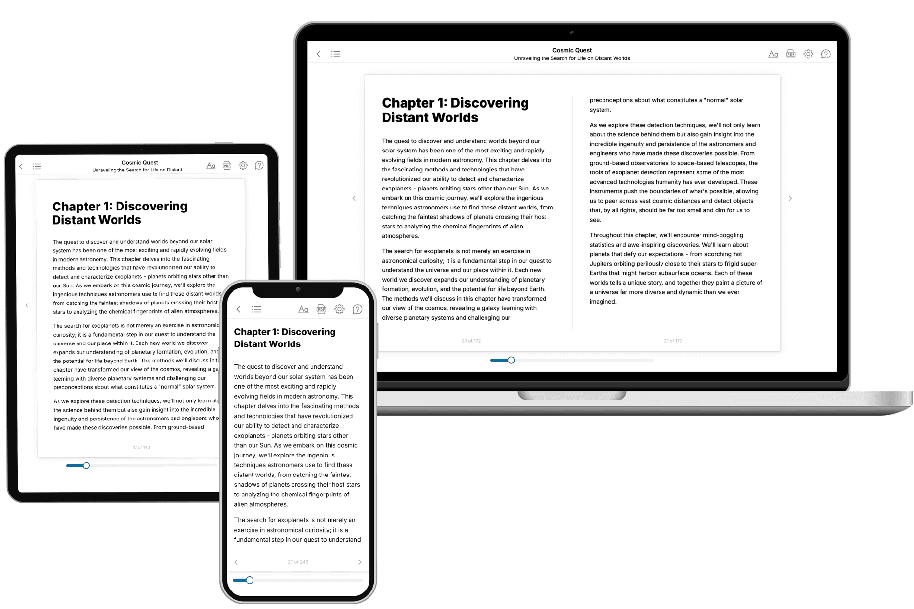
TailoredRead creates complete, full-length nonfiction ebooks, written specifically for you. Tell us what you want to learn and why, and TailoredRead writes you a complete ebook on it, with charts, tables, and diagrams throughout. Read it online, on Kindle, or on any e-reader, or download it as a PDF or EPUB. Every book is written fresh the day you order it.
- How is the book tailored to me?
Before anything is written, you answer a few short questions about your goals, your background, and the topics you care about. Your book is then planned around your answers: written at your level, focused on your goals, and covering the topics you chose, instead of the one-size-fits-all book a store sells everyone.
- Will it read like generic AI content?
No. Your book isn't a chat transcript: it's planned chapter by chapter before a single word is written, told in a clear book voice, and explains ideas visually with charts, tables, and diagrams. After writing, every book goes through an editorial pass that polishes chapters so the book reads consistent from start to finish. Judge for yourself: browse thousands of sample books on our Explore Books page.
- How accurate is the content?
Our AI first checks whether your subject needs live research. Niche and fast-moving subjects are researched before writing, and the book plan and chapters are grounded in what it finds. After writing, every book goes through a quality pass that checks its facts and consistency, and researched books list their sources in a Notes section at the back.
- How long is the book?
You choose the length: Comprehensive (250-300 pages), Detailed (150-200 pages), Essential (70-100 pages), or Short (30-50 pages).
- Does the book include visuals?
Yes. Every book includes charts, tables, and diagrams: timelines, checklists, step-by-step guides, decision trees, comparison tables, matrices, and bar charts. A typical book includes dozens of these visual elements.
- Can I read it on Kindle? What formats can I download?
Yes. Every book can be read in our online reader or downloaded as a PDF or EPUB. The EPUB can be opened with Kindle, Apple Books, Kobo, and any e-reader. The Commercial and Author licenses also include an editable Word (DOCX) and Markdown download.
- How much does it cost?
About the price of a regular ebook. The exact price depends on your book's length and complexity, from $2 for the shortest books to $35 for the most comprehensive, and it's shown when you review your book, before you commit to anything. Each book is a one-time purchase, yours to keep, no subscription. Licenses that let you share, teach, or publish your book range from $35.99 to $49.99.
- Can I preview the book before purchasing?
Before you pay, you'll see what your book will cover: the title, a detailed description, the estimated length, and the complete chapter-by-chapter table of contents, so you know what you're getting before you decide. The full text itself is written after you purchase.
- How long does it take to create a book?
About 10 minutes. You can start reading the opening chapters while the rest is still being written.